ZHCSKU1A February   2020  – July 2020 2N7001T-Q1

PRODUCTION DATA  

  1. 特性
  2. 应用
  3. 说明
  4. Revision History
  5. Pin Configuration and Functions
    1.     6
  6. Specifications
    1. 6.1 Absolute Maximum Ratings
    2. 6.2 ESD Ratings
    3. 6.3 Recommended Operating Conditions
    4. 6.4 Thermal Information
    5. 6.5 Electrical Characteristics
    6. 6.6 Switching Characteristics
    7. 6.7 Operating Characteritics: TA = 25°C
    8. 6.8 Typical Characteristics
  7. Parameter Measurement Information
    1. 7.1 Load Circuit and Voltage Waveforms
  8. Detailed Description
    1. 8.1 Overview
    2. 8.2 Functional Block Diagram
    3. 8.3 Feature Description
      1. 8.3.1 Up-Translation or Down-Translation from 1.65 V to 3.60 V
      2. 8.3.2 Balanced CMOS Push-Pull Outputs
      3. 8.3.3 Standard CMOS Inputs
      4. 8.3.4 Negative Clamping Diodes
      5. 8.3.5 Partial Power Down (Ioff)
      6. 8.3.6 Over-voltage Tolerant Inputs
    4. 8.4 Device Functional Modes
  9. Application and Implementation
    1. 9.1 Application Information
    2. 9.2 Typical Applications
      1. 9.2.1 Processor Error Up Translation
        1. 9.2.1.1 Design Requirements
        2. 9.2.1.2 Detailed Design Procedure
        3. 9.2.1.3 Application Curve
      2. 9.2.2 Discrete FET Translation Replacement
  10. 10Power Supply Recommendations
  11. 11Layout
    1. 11.1 Layout Guidelines
    2. 11.2 Layout Example
  12. 12Device and Documentation Support
    1. 12.1 Documentation Support
      1. 12.1.1 Related Documentation
    2. 12.2 Receiving Notification of Documentation Updates
    3. 12.3 Support Resources
    4. 12.4 Trademarks
    5. 12.5 Electrostatic Discharge Caution
    6. 12.6 Glossary
  13. 13Mechanical, Packaging, and Orderable Information

封装选项

机械数据 (封装 | 引脚)
散热焊盘机械数据 (封装 | 引脚)
订购信息

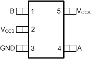
Pin Configuration and Functions

GUID-60F431E3-A009-4314-82E4-BBA57ACB163E-low.gif Figure 5-1 DCK Package5-Pin SC70Top View