SNOSBI1C November 2009 – June 2015
PRODUCTION DATA.
- 1 Features
- 2 Applications
- 3 Description
- 4 Revision History
- 5 Pin Configuration and Functions
- 6 Specifications
- 7 Parameter Measurement Information
- 8 Detailed Description
-
9 Application and Implementation
- 9.1 Application Information
- 9.2
Typical Applications
- 9.2.1
8080 Interface
- 9.2.1.1 Design Requirements
- 9.2.1.2
Detailed Design Procedure
- 9.2.1.2.1 Analog Differential Voltage Inputs and Common-Mode Rejection
- 9.2.1.2.2 Analog Inputs — Input Current
- 9.2.1.2.3 Reference Voltage
- 9.2.1.2.4 Errors and Reference Voltage Adjustments
- 9.2.1.2.5 Clocking Option
- 9.2.1.2.6 Restart During a Conversion
- 9.2.1.2.7 Continuous Conversions
- 9.2.1.2.8 Driving the Data Bus
- 9.2.1.2.9 Wiring and Hook-Up Precautions
- 9.2.2 Multiple ADC0801 Series to MC6800 CPU Interface
- 9.2.3 Auto-Zeroed Differential Transducer Amplifier and ADC Converter
- 9.2.4 Multiple ADC Converters in a Z-80 Interrupt Driven Mode
- 9.2.1
8080 Interface
- 9.3 System Examples
- 10Power Supply Recommendations
- 11Layout
- 12Device and Documentation Support
- 13Mechanical, Packaging, and Orderable Information
8 Detailed Description
8.1 Overview
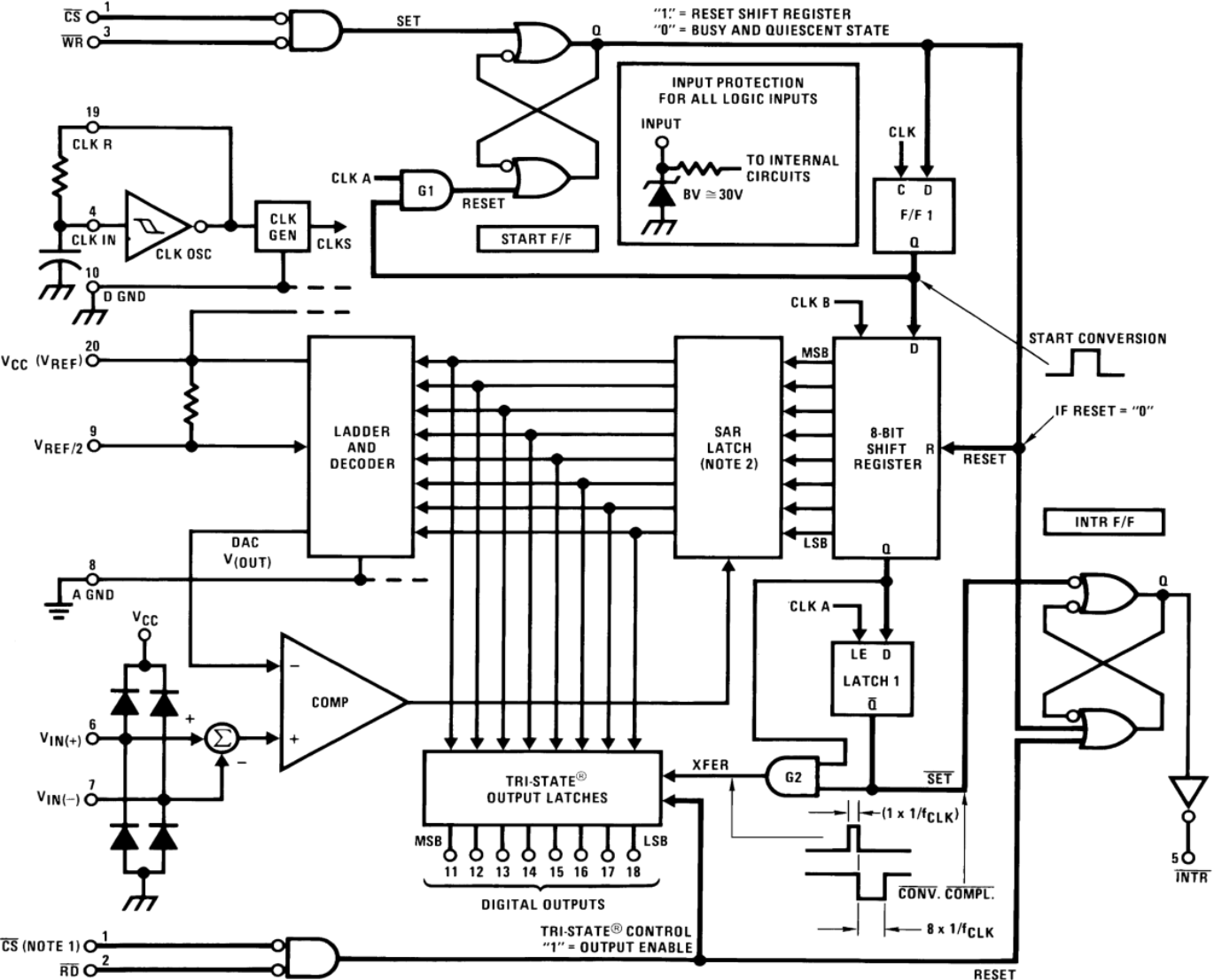
The ADC0801 series are versatile 8-Bit µP compatible general purpose ADC converters operate on single 5-V supply. These devices are treated as a memory location or I/O port to a micro-processor system without additional interface logic. The outputs are Tri-state latched which facilitate interfacing to micro-processor control bus. The converter is designed with a differential potentiometric ladder, a circuit equivalent of the 256R network. It contains analog switches sequenced by successive approximation logic. A functional diagram of the ADC converter is shown in Functional Block Diagram. All of the package pinouts are shown and the major logic control paths are drawn in heavier weight lines. The differential analog voltage input has good common mode-rejection and permits offsetting the analog zero-input voltage value. Moreover, the input reference voltage can be adjusted to allow encoding small analog voltage span to the full 8-bits resolution. To ensure start-up under all possible conditions, an external WR pulse is required during the first power-up cycle.
Using a SAR logic the most significant bit is tested first and after 8 comparisons (64 clock cycles) a digital 8-bit binary code (1111 1111 = full-scale) is transferred to an output latch and then an interrupt is asserted (INTR makes a high-to-low transition). A conversion in process can be interrupted by issuing a second start command. The device may be operated in the free-running mode by connecting INTR to the WR input with CS=0.
On the high-to-low transition of the WR input the internal SAR latches and the shift register stages are reset. As long as the CS input and WR input remain low, the ADC will remain in a reset state. Conversion will start from 1 to 8 clock periods after at least one of these inputs makes a low-to-high transition.
The converter is started by having CS and WR simultaneously low. This sets the start flip-flop (F/F) and the resulting “1” level resets the 8-bit shift register, resets the Interrupt (INTR) F/F and inputs a “1” to the D flop, F/F1, which is at the input end of the 8-bit shift register. Internal clock signals then transfer this “1” to the Q output of F/F1. The AND gate, G1, combines this “1” output with a clock signal to provide a reset signal to the start F/F. If the set signal is no longer present (either WR or CS is a “1”) the start F/F is reset and the 8-bit shift register then can have the “1” clocked in, which starts the conversion process. If the set signal were to still be present, this reset pulse would have no effect (both outputs of the start F/F would momentarily be at a “1” level) and the 8-bit shift register would continue to be held in the reset mode. This logic therefore allows for wide CS and WR signals and the converter will start after at least one of these signals returns high and the internal clocks again provide a reset signal for the start F/F.
After the “1” is clocked through the 8-bit shift register (which completes the SAR search) it appears as the input to the D-type latch, LATCH 1. As soon as this “1” is output from the shift register, the AND gate, G2, causes the new digital word to transfer to the Tri-state output latches. When LATCH 1 is subsequently enabled, the Q output makes a high-to-low transition which causes the INTR F/F to set. An inverting buffer then supplies the INTR input signal.
Note this SET control of the INTR F/F remains low for 8 of the external clock periods (as the internal clocks run at 1/8 of the frequency of the external clock). If the data output is continuously enabled (CS and RD both held low), the INTR output will still signal the end of conversion (by a high-to-low transition), because the SET input can control the Q output of the INTR F/F even though the RESET input is constantly at a M "1M " level in this operating mode. This INTR output will therefore stay low for the duration of the SET signal, which is 8 periods of the external clock frequency (assuming the ADC is not started during this interval).
When operating in the free-running or continuous conversion mode (INTR pin tied to WR and CS wired low – see Continuous Conversions), the START F/F is SET by the high-to-low transition of the INTR signal. This resets the SHIFT REGISTER which causes the input to the D-type latch, LATCH 1, to go low. As the latch enable input is still present, the Q output will go high, which then allows the INTR F/F to be RESET. This reduces the width of the resulting INTR output pulse to only a few propagation delays (approximately 300 ns).
When data is to be read, the combination of both CS and RD being low will cause the INTR F/F to be reset and the Tri-state output latches will be enabled to provide the 8-bit digital outputs.
8.2 Functional Block Diagram
8.3 Feature Description
8.3.1 Understanding ADC Error Specs
A perfect ADC transfer characteristic (staircase waveform) is shown in Figure 16 and Figure 17. The horizontal scale is analog input voltage and the particular points labeled are in steps of 1 LSB (19.53 mV with 2.5V tied to the VREF/2 pin). The digital output codes that correspond to these inputs are shown as D−1, D, and D+1. For the perfect ADC, not only will center- value (A−1, A, A+1, . . . . ) analog inputs produce the cor- rect output digital codes, but also each riser (the transitions between adjacent output codes) will be located ±1⁄2 LSB away from each center-value. As shown, the risers are ideal and have no width. Correct digital output codes will be provided for a range of analog input voltages that extend ±1⁄2 LSB from the ideal center-values. Each tread (the range of analog input voltage that provides the same digital output code) is therefore 1 LSB wide.
Figure 19 shows a worst case error plot for the ADC0801. All center-valued inputs are guaranteed to produce the correct output codes and the adjacent risers are specified to be no closer to the center-value points than ±1/4 LSB. In other words, if we apply an analog input equal to the center-value ±1/4 LSB, we guarantee that the ADC will produce the correct digital code. The maximum range of the position of the code transition is indicated by the horizontal arrow and it is specified to be no more than 1/2 LSB.
The error curve of Figure 21 shows a worst case error plot for the ADC0802. Here we guarantee that if we apply an analog input equal to the LSB analog voltage center-value the ADC will produce the correct digital code.
Next to each transfer function is shown the corresponding error plot. Many people may be more familiar with error plots than transfer functions. The analog input voltage to the ADC is provided by either a linear ramp or by the discrete output steps of a high resolution DAC. Notice that the error is continuously displayed and includes the quantization uncertainty of the ADC. For example the error at point 1 of Figure 21 is +1⁄2 LSB because the digital code appeared 1⁄2 LSB in advance of the center-value of the tread. The error plots always have a constant negative slope and the abrupt up-side steps are always 1 LSB in magnitude.
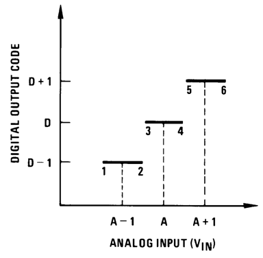 Figure 16. Transfer Function of Analog Input vs Digital Output Code in Ideal ADC
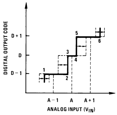 Figure 18. Transfer Function of Analog Input vs Digital Output Code for ±1/4 LSB Accuracy ADC
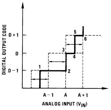 Figure 20. Transfer Function of Analog Input vs Digital Output Code for ±1/2 LSB Accuracy ADC
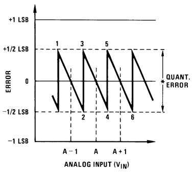 Figure 17. Clarifying the Error Specs of an ADC Converter Accuracy=±0 LSB: A Perfect ADC
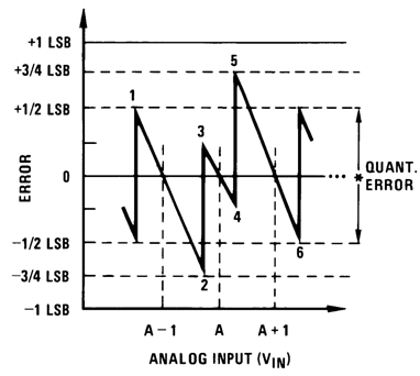 Figure 19. Clarifying the Error Specs of an ADC Converter Accuracy =±1⁄4 LSB
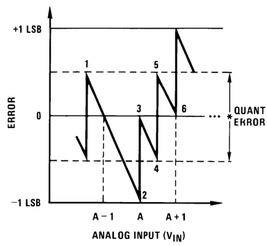 Figure 21. Clarifying the Error Specs of an ADC Converter Accuracy = ±1⁄2 LSB
8.3.2 Digital Control Inputs
The digital control inputs (CS, RD, and WR) meet standard TLL logic voltage levels. These signals have been renamed when compared to the standard ADC Start and Output Enable labels. In addition, these inputs are active low to allow an easy interface to microprocessor control busses. For non-microprocessor based applications, the CS input (pin 1) can be grounded and the standard ADC Start function is obtained by an active low pulse applied at the WR input (pin 3) and the Output Enable function is caused by an active low pull at the RD input (pin 2).
8.4 Device Functional Modes
8.4.1 Analog Input Modes
8.4.1.1 Normal Mode
Due to the internal switching action, displacement currents will flow at the analog inputs. This is due to on-chip stray capacitance to ground as shown in Figure 22.
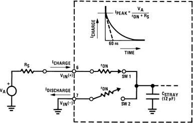
r=rON CSTRAY × 5 kΩ x 12 pF = 60 ns
The voltage on this capacitance is switched and will result in currents entering the VIN(+) input pin and leaving the VIN(−) input which will depend on the analog differential input voltage levels. These current transients occur at the leading edge of the internal clocks. They rapidly decay and do not cause errors as the on-chip comparator is strobed at the end of the clock period.
8.4.1.2 Fault Mode
If the voltage source applied to the VIN(+) or VIN(−) pin exceeds the allowed operating range of VCC+50 mV, large input currents can flow through a parasitic diode to the VCC pin. If these currents can exceed the 1 mA max allowed spec, an external diode (1N914) should be added to bypass this current to the VCC pin (with the current bypassed with this diode, the voltage at the VIN(+) pin can exceed the VCC voltage by the forward voltage of this diode).