SNOSBI1C
November 2009 – June 2015
PRODUCTION DATA.
1
Features
2
Applications
3
Description
4
Revision History
5
Pin Configuration and Functions
6
Specifications
6.1
Absolute Maximum Ratings
6.2
ESD Ratings
6.3
Recommended Operating Conditions
6.4
Thermal Information
6.5
Operating Ratings
6.6
Electrical Characteristics
6.7
AC Electrical Characteristics
6.8
Typical Characteristics
7
Parameter Measurement Information
7.1
Tri-State Test Circuits and Waveforms
8
Detailed Description
8.1
Overview
8.2
Functional Block Diagram
8.3
Feature Description
8.3.1
Understanding ADC Error Specs
8.3.2
Digital Control Inputs
8.4
Device Functional Modes
8.4.1
Analog Input Modes
8.4.1.1
Normal Mode
8.4.1.2
Fault Mode
9
Application and Implementation
9.1
Application Information
9.1.1
Testing the ADC Converter
9.1.2
Microprocessor Interfacing
9.1.2.1
Interfacing 8080 Microprocessor Derivatives (8048, 8085)
9.1.2.2
Sample 8080A CPU Interfacing Circuitry and Program
9.1.2.3
INS8048 Interface
9.1.2.4
Interfacing the Z-80
9.1.2.5
Interfacing 6800 Microprocessor Derivatives (6502, etc.)
9.2
Typical Applications
9.2.1
8080 Interface
9.2.1.1
Design Requirements
9.2.1.2
Detailed Design Procedure
9.2.1.2.1
Analog Differential Voltage Inputs and Common-Mode Rejection
9.2.1.2.2
Analog Inputs — Input Current
9.2.1.2.2.1
Input Bypass Capacitors
9.2.1.2.2.2
Input Source Resistance
9.2.1.2.2.3
Noise
9.2.1.2.3
Reference Voltage
9.2.1.2.3.1
Span Adjust
9.2.1.2.3.2
Reference Accuracy Requirements
9.2.1.2.4
Errors and Reference Voltage Adjustments
9.2.1.2.4.1
Zero Error
9.2.1.2.4.2
Full-Scale
9.2.1.2.4.3
Adjusting for an Arbitrary Analog Input Voltage Range
9.2.1.2.5
Clocking Option
9.2.1.2.6
Restart During a Conversion
9.2.1.2.7
Continuous Conversions
9.2.1.2.8
Driving the Data Bus
9.2.1.2.9
Wiring and Hook-Up Precautions
9.2.2
Multiple ADC0801 Series to MC6800 CPU Interface
9.2.3
Auto-Zeroed Differential Transducer Amplifier and ADC Converter
9.2.4
Multiple ADC Converters in a Z-80 Interrupt Driven Mode
9.3
System Examples
10
Power Supply Recommendations
11
Layout
11.1
Layout Guidelines
12
Device and Documentation Support
12.1
Related Links
12.2
Community Resources
12.3
Trademarks
12.4
Electrostatic Discharge Caution
12.5
Glossary
13
Mechanical, Packaging, and Orderable Information
封装选项
机械数据 (封装 | 引脚)
DW|20
MPDS173B
散热焊盘机械数据 (封装 | 引脚)
订购信息
snosbi1c_oa
snosbi1c_pm
7 Parameter Measurement Information
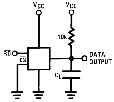
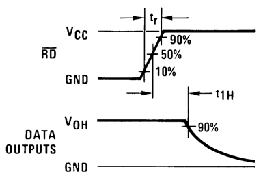
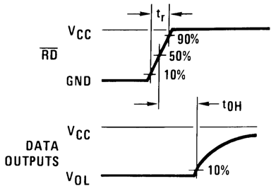
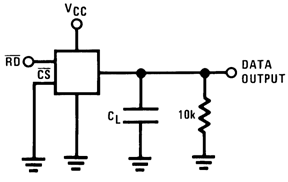
7.1 Tri-State Test Circuits and Waveforms
C
L
= 10 pF
Figure 12. RD to Data Output Falling Edge Test Load Condition
C
L
= 10 pF
Figure 14. RD to Data Output Rising Edge Test Load Condition
Figure 13. RD to Data Output Falling Edge Test Timing
Figure 15. RD to Data Output Rising Edge Test Timing
千亿体育app官网登录(中国)官方网站IOS/安卓通用版/手机APP
|
米乐app下载官网(中国)|ios|Android/通用版APP最新版
|
米乐|米乐·M6(中国大陆)官方网站
|
千亿体育登陆地址
|
华体会体育(中国)HTH·官方网站
|
千赢qy国际_全站最新版千赢qy国际V6.2.14安卓/IOS下载
|
18新利网v1.2.5|中国官方网站
|
bob电竞真人(中国官网)安卓/ios苹果/电脑版【1.97.95版下载】
|
千亿体育app官方下载(中国)官方网站IOS/安卓/手机APP下载安装
|