SNAS279F April 2005 – July 2016 ADC084S021
PRODUCTION DATA.
- 1 Features
- 2 Applications
- 3 Description
- 4 Revision History
- 5 Device Comparison Table
- 6 Pin Configuration and Functions
- 7 Specifications
- 8 Detailed Description
- 9 Application and Implementation
- 10Power Supply Recommendations
- 11Layout
- 12Device and Documentation Support
- 13Mechanical, Packaging, and Orderable Information
9 Application and Implementation
NOTE
Information in the following applications sections is not part of the TI component specification, and TI does not warrant its accuracy or completeness. TI’s customers are responsible for determining suitability of components for their purposes. Customers should validate and test their design implementation to confirm system functionality.
9.1 Application Information
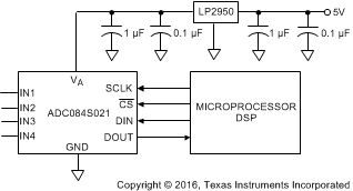
Figure 49 shows a typical application of the ADC084S021. Power is provided, in this example, by the Texas Instruments LP2950 low-dropout voltage regulator, available in a variety of fixed and adjustable output voltages. The power supply pin is bypassed with a capacitor network located close to the ADC084S021.
Because the reference for the ADC084S021 is the supply voltage, any noise on the supply degrades device noise performance. Use a dedicated linear regulator for this device, or provide sufficient decoupling from other circuitry to keep noise off the ADC084S021 supply pin. Because of the low power requirements of the ADC084S021, it is also possible to use a precision reference as a power supply to maximize performance. The four-wire interface is also shown connected to a microprocessor or DSP.
9.2 Typical Application
 Figure 49. Typical Application Circuit
9.2.1 Design Requirements
In this application, the power consumption of the ADC084S021 must not exceed 1 mW and the throughput may range from 50 ksps to 200 ksps.
9.2.2 Detailed Design Procedure
The two largest factors that impact the power consumption of the ADC084S021 are the supply voltage and the throughput. According to Figure 50, a supply voltage of 3 V allows a throughput of up to 200 ksps at less than
1-mW power consumption. If a supply voltage of 5 V is chosen then the maximum throughput achievable is about 40 ksps, which does not meet the design requirements. Select a supply voltage of 3 V with a FCLK of
3.2 MHz to meet all of the design requirements.
9.2.3 Application Curve
 Figure 50. Power Consumption vs Throughput