ZHCSN42A August   2021  – May 2022 ADC08DJ5200RF

PRODUCTION DATA  

  1. 特性
  2. 应用
  3. 说明
  4. Revision History
  5. Pin Configuration and Functions
  6. Specifications
    1. 6.1  Absolute Maximum Ratings
    2. 6.2  ESD Ratings
    3. 6.3  Recommended Operating Conditions
    4. 6.4  Thermal Information
    5. 6.5  Electrical Characteristics: DC Specifications
    6. 6.6  Electrical Characteristics: Power Consumption
    7. 6.7  Electrical Characteristics: AC Specifications (Dual-Channel Mode)
    8. 6.8  Electrical Characteristics: AC Specifications (Single-Channel Mode)
    9. 6.9  Timing Requirements
    10. 6.10 Switching Characteristics
    11. 6.11 Typical Characteristics
  7. Detailed Description
    1. 7.1 Overview
    2. 7.2 Functional Block Diagram
    3. 7.3 Feature Description
      1. 7.3.1 Device Comparison
      2. 7.3.2 Analog Inputs
        1. 7.3.2.1 Analog Input Protection
        2. 7.3.2.2 Full-Scale Voltage (VFS) Adjustment
        3. 7.3.2.3 Analog Input Offset Adjust
      3. 7.3.3 ADC Core
        1. 7.3.3.1 ADC Theory of Operation
        2. 7.3.3.2 ADC Core Calibration
        3. 7.3.3.3 Analog Reference Voltage
        4. 7.3.3.4 ADC Overrange Detection
        5. 7.3.3.5 Code Error Rate (CER)
      4. 7.3.4 Temperature Monitoring Diode
      5. 7.3.5 Timestamp
      6. 7.3.6 Clocking
        1. 7.3.6.1 Noiseless Aperture Delay Adjustment (tAD Adjust)
        2. 7.3.6.2 Aperture Delay Ramp Control (TAD_RAMP)
        3. 7.3.6.3 SYSREF Capture for Multi-Device Synchronization and Deterministic Latency
          1. 7.3.6.3.1 SYSREF Position Detector and Sampling Position Selection (SYSREF Windowing)
          2. 7.3.6.3.2 Automatic SYSREF Calibration
      7. 7.3.7 Programmable FIR Filter (PFIR)
        1. 7.3.7.1 Dual Channel Equalization
        2. 7.3.7.2 Single Channel Equalization
        3. 7.3.7.3 Time Varying Filter
      8. 7.3.8 JESD204C Interface
        1. 7.3.8.1 Transport Layer
        2. 7.3.8.2 Scrambler
        3. 7.3.8.3 Link Layer
        4. 7.3.8.4 8B/10B Link Layer
          1. 7.3.8.4.1 Data Encoding (8B/10B)
          2. 7.3.8.4.2 Multiframes and the Local Multiframe Clock (LMFC)
          3. 7.3.8.4.3 Code Group Synchronization (CGS)
          4. 7.3.8.4.4 Initial Lane Alignment Sequence (ILAS)
          5. 7.3.8.4.5 Frame and Multiframe Monitoring
        5. 7.3.8.5 64B/66B Link Layer
          1. 7.3.8.5.1 64B/66B Encoding
          2. 7.3.8.5.2 Multiblocks, Extended Multiblocks and the Local Extended Multiblock Clock (LEMC)
          3. 7.3.8.5.3 Block, Multiblock and Extended Multiblock Alignment using Sync Header
            1. 7.3.8.5.3.1 Cyclic Redundancy Check (CRC) Mode
            2. 7.3.8.5.3.2 Forward Error Correction (FEC) Mode
          4. 7.3.8.5.4 Initial Lane Alignment
          5. 7.3.8.5.5 Block, Multiblock and Extended Multiblock Alignment Monitoring
        6. 7.3.8.6 Physical Layer
          1. 7.3.8.6.1 SerDes Pre-Emphasis
        7. 7.3.8.7 JESD204C Enable
        8. 7.3.8.8 Multi-Device Synchronization and Deterministic Latency
        9. 7.3.8.9 Operation in Subclass 0 Systems
      9. 7.3.9 Alarm Monitoring
        1. 7.3.9.1 Clock Upset Detection
        2. 7.3.9.2 FIFO Upset Detection
    4. 7.4 Device Functional Modes
      1. 7.4.1 Dual-Channel Mode
      2. 7.4.2 Single-Channel Mode (DES Mode)
      3. 7.4.3 Dual-Input Single-Channel Mode (DUAL DES Mode)
      4. 7.4.4 JESD204C Modes
        1. 7.4.4.1 JESD204C Operating Modes Table
        2. 7.4.4.2 JESD204C Modes continued
        3. 7.4.4.3 JESD204C Transport Layer Data Formats
        4. 7.4.4.4 64B/66B Sync Header Stream Configuration
      5. 7.4.5 Power-Down Modes
      6. 7.4.6 Test Modes
        1. 7.4.6.1 Serializer Test-Mode Details
        2. 7.4.6.2 PRBS Test Modes
        3. 7.4.6.3 Clock Pattern Mode
        4. 7.4.6.4 Ramp Test Mode
        5. 7.4.6.5 Short and Long Transport Test Mode
          1. 7.4.6.5.1 Short Transport Test Pattern
        6. 7.4.6.6 D21.5 Test Mode
        7. 7.4.6.7 K28.5 Test Mode
        8. 7.4.6.8 Repeated ILA Test Mode
        9. 7.4.6.9 Modified RPAT Test Mode
      7. 7.4.7 Calibration Modes and Trimming
        1. 7.4.7.1 Foreground Calibration Mode
        2. 7.4.7.2 Background Calibration Mode
        3. 7.4.7.3 Low-Power Background Calibration (LPBG) Mode
      8. 7.4.8 Offset Calibration
      9. 7.4.9 Trimming
    5. 7.5 Programming
      1. 7.5.1 Using the Serial Interface
        1. 7.5.1.1 SCS
        2. 7.5.1.2 SCLK
        3. 7.5.1.3 SDI
        4. 7.5.1.4 SDO
        5. 7.5.1.5 Streaming Mode
    6. 7.6 SPI Register Map
  8. Application Information Disclaimer
    1. 8.1 Application Information
    2. 8.2 Typical Applications
      1. 8.2.1 Reconfigurable Dual-Channel 5-GSPS or Single-Channel 10-Gsps Oscilloscope
        1. 8.2.1.1 Design Requirements
          1. 8.2.1.1.1 Input Signal Path
          2. 8.2.1.1.2 Clocking
          3. 8.2.1.1.3 ADC08DJ5200RF
    3. 8.3 Initialization Set Up
  9. Power Supply Recommendations
    1. 9.1 Power Sequencing
  10. 10Layout
    1. 10.1 Layout Guidelines
    2. 10.2 Layout Example
  11. 11Device and Documentation Support
    1. 11.1 Device Support
      1. 11.1.1 Development Support
        1. 11.1.1.1 123
    2. 11.2 Documentation Support
      1. 11.2.1 Related Documentation
    3. 11.3 Receiving Notification of Documentation Updates
    4. 11.4 Support Resources
    5. 11.5 Trademarks
    6. 11.6 Electrostatic Discharge Caution
    7. 11.7 术语表
  12. 12Mechanical, Packaging, and Orderable Information

封装选项

机械数据 (封装 | 引脚)
散热焊盘机械数据 (封装 | 引脚)
订购信息

Power Supply Recommendations

The device requires two different power-supply voltages. 1.9-V DC is required for the VA19 power bus and 1.1-V DC is required for the VA11 and VD11 power buses.

The power-supply voltages must be low noise and provide the needed current to achieve rated device performance.

There are two recommended power supply architectures:

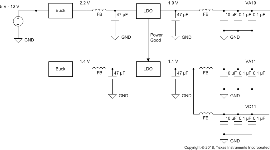
  1. Step down using high-efficiency switching converters, followed by a second stage of regulation to provide switching noise reduction and improved voltage accuracy.
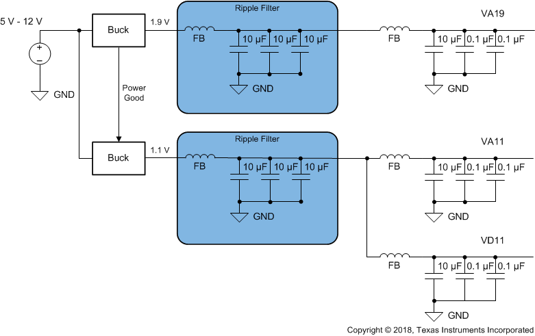
  2. Directly step down the final ADC supply voltage using high-efficiency switching converters. This approach provides the best efficiency, but care must be taken for switching noise to be minimized to prevent degraded ADC performance.

TI WEBENCH® Power Designer can be used to select and design the individual power supply elements needed: see the WEBENCH® Power Designer

Recommended switching regulators for the first stage include LMS3635-Q1, LMS3655-Q1, TPSM84424 and similar devices.

Recommended low drop-out (LDO), low-noise linear regulators include the TPS7A84, TPS7A83A, TPS7A47 and similar devices.

For the switcher only approach, the ripple filter must be designed to provide sufficient filtering at the switching frequency of the DC-DC converter and harmonics of the switching frequency. Make a note of the switching frequency reported from WEBENCH® and design the EMI filter and capacitor combination to have the notch frequency centered as needed. Each application will have different tolerances for noise on the supply voltage so strict ripple requirements are not provided. Figure 9-1 and Figure 9-2 illustrate the two approaches.
GUID-F061F376-C277-4342-BB50-6A61E2109DAC-low.gif
FB = ferrite bead filter.
Figure 9-1 LDO Linear Regulator Approach Example
GUID-70933BEC-424E-421C-A460-4F72CD4C18CC-low.gif
Ripple filter notch frequency to match the fs of the buck converter.
FB = ferrite bead filter.
Figure 9-2 Switcher-Only Approach Example