Typical values at 25°C, AIN
= -1 dBFS, FIN = 347 MHz, FS = 1300 MSPS, High power mode, FG
calibration, JMODE 0, CPLL off, CPLLREF = 50 MHz and VA11Q and VCLK11
noise suppression on when CPLL on, nominal supply voltages, unless otherwise noted.
SNR results exclude DC, HD2 to HD9; SINAD, ENOB, and SFDR results exclude DC.
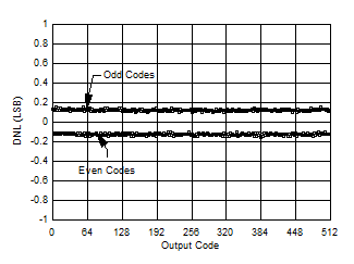
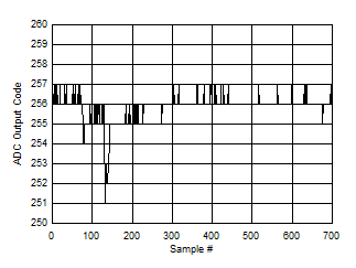
 Figure 5-1 DNL
vs Code
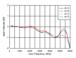
 Figure 5-3 Input
Fullscale vs Input Frequency
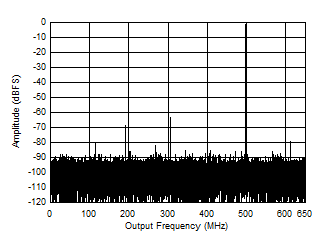
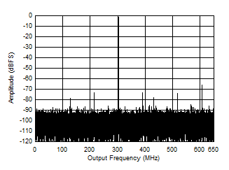
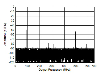
 Figure 5-5 Single Tone FFT at 497 MHz and -1 dBFS
 Figure 5-7 Single Tone FFT at 1497 MHz and -1 dBFS
 Figure 5-9 Single Tone FFT at 2697 MHz and -1 dBFS
| FS = 1000MSPS, Low Power Mode |
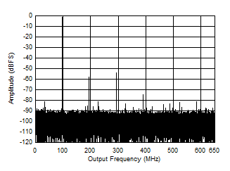
Figure 5-11 Single Tone FFT at 99.997 MHz and -1 dBFS
| FS = 1000MSPS, Low Power Mode |
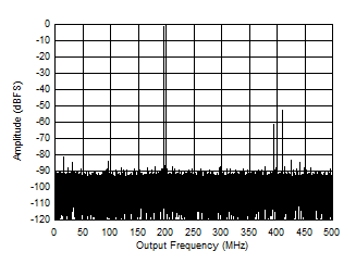
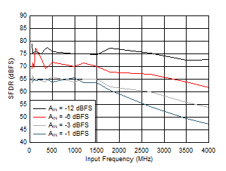
Figure 5-13 Single Tone FFT at 1197 MHz and -1 dBFS Figure 5-15 SFDR vs Input Frequency
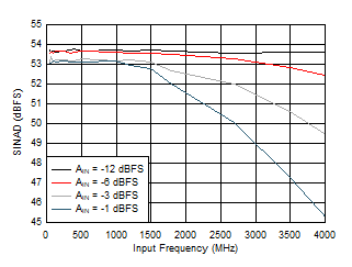
 Figure 5-17 SINAD vs Input Frequency
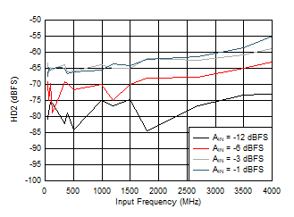
 Figure 5-19 HD2 vs Input Frequency
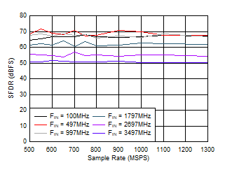
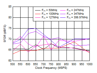
 Figure 5-21 SFDR vs Sample Rate
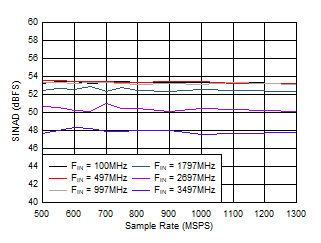
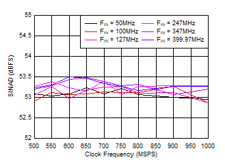
 Figure 5-23 SINAD vs Sample Rate
| FS = 1000MSPS, Low Power Mode |
Figure 5-25 SFDR vs Sample Rate
| FS = 1000MSPS, Low Power Mode |
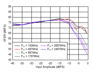
Figure 5-27 SINAD vs Sample Rate Figure 5-29 SFDR vs Input Amplitude
| FS = 1000MSPS, FIN =
100MHz,Low Power Mode |
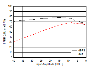
Figure 5-31 SFDR vs Input Amplitude Figure 5-33 SFDR
vs Clock Amplitude
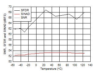
 Figure 5-35 SNR, SFDR and SINAD vs Temperature
| FIN = 997 MHz, FG25°C means calibration
at 25°C and held across temperature |
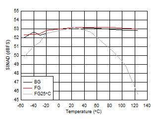
Figure 5-37 SINAD vs Temperature and Calibration Mode
| FIN = 997 MHz, FG25°C means calibration
at 25°C and held across temperature |
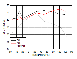
Figure 5-39 SFDR vs Temperature and Calibration Mode
| Low
Power Mode, FIN = 347 MHz, FG25°C means
calibration at 25°C and held across temperature |
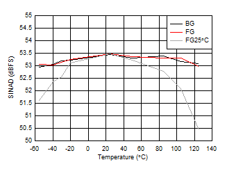
Figure 5-41 SINAD vs Temperature and Calibration Mode
| Low
Power Mode, FIN = 347 MHz, FG25°C means
calibration at 25°C and held across temperature |
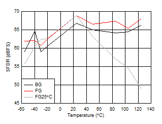
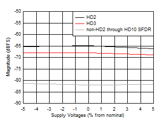
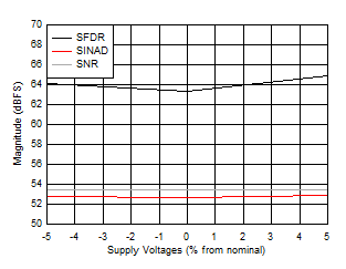
Figure 5-43 SFDR vs Temperature and Calibration Mode Figure 5-45 HD2, HD3 and Worst non-HD Spur vs Supply
Voltage
| Low
Power Mode, FIN = 347 MHz, FS =
1000MSPS |
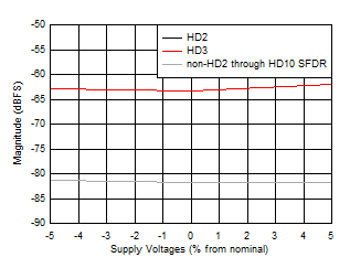
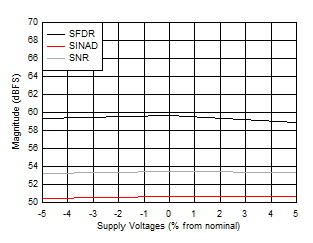
Figure 5-47 HD2, HD3 and Worst non-HD Spur vs Supply
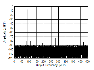
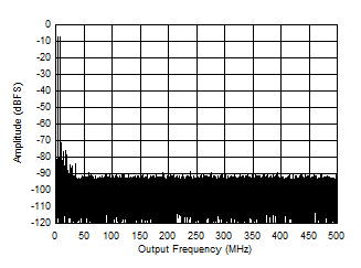
Voltage Figure 5-49 Two
Tone FFT at 348 MHz Center
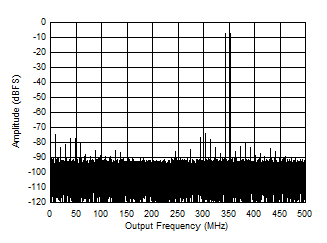
 Figure 5-51 Two
Tone FFT at 998 MHz Center
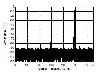
 Figure 5-53 Two
Tone FFT at 2698 MHz Center
| Low
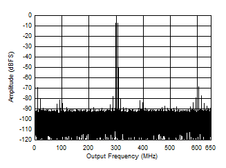
Power Mode, FS = 1000 MSPS, 10 MHz Tone
Spacing |
Figure 5-55 Two
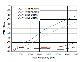
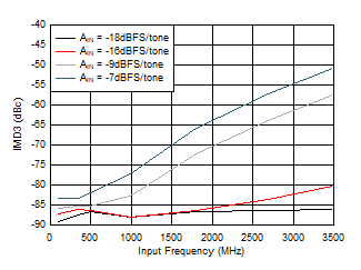
Tone FFT at 348 MHz Center Figure 5-57 IMD3 vs Input Frequency
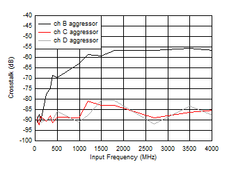
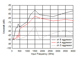
 Figure 5-59 Crosstalk to Channel A vs FIN
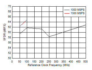
 Figure 5-61 SFDR vs Reference Clock Frequency
| FS = 1300MSPS, High Power Mode |
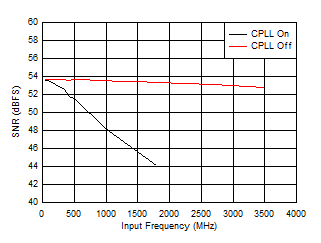
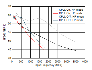
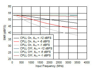
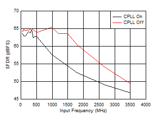
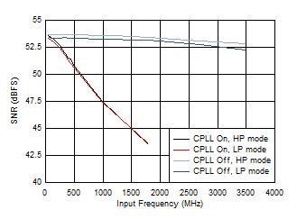
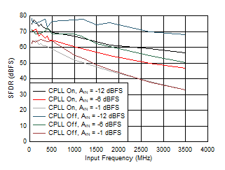
Figure 5-63 SNR vs Input Frequency and CPLL Figure 5-65 SFDR vs Input Frequency and CPLL
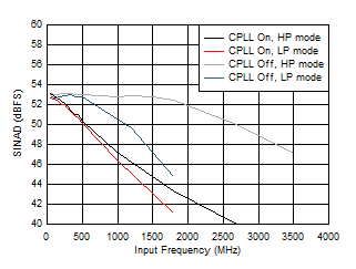
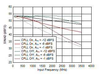
 Figure 5-67 SINAD vs Input Frequency and CPLL
| FS = 1300MSPS, High Power Mode |
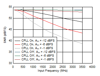
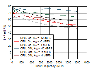
Figure 5-69 SNR vs Input Frequency, CPLL and Input
Amplitude
| FS = 1300MSPS, High Power Mode |
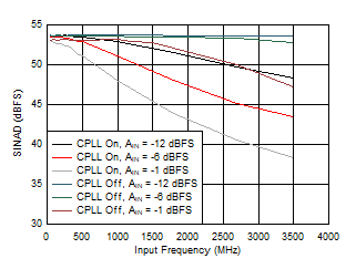
Figure 5-71 SINAD vs Input Frequency, CPLL and Input
Amplitude
| FS = 1300MSPS, High Power Mode |
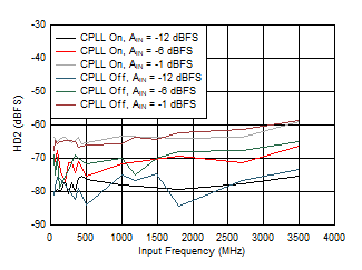
Figure 5-73 HD2 vs Input Frequency, CPLL and Input
Amplitude
| FS = 1000MSPS, Low Power Mode |
Figure 5-75 SNR vs Input Frequency, CPLL and Input
Amplitude
| FS = 1000MSPS, Low Power Mode |
Figure 5-77 SINAD vs Input Frequency, CPLL and Input
Amplitude
| FS = 1000MSPS, Low Power Mode |
Figure 5-79 HD2 vs Input Frequency, CPLL and Input
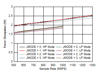
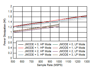
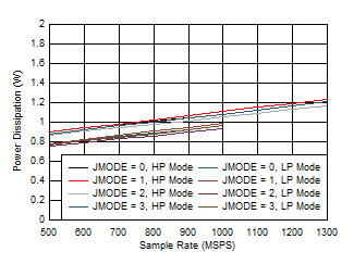
Amplitude Figure 5-81 Quad Channel, Power Dissipation vs FS for JMODES 0 -
3
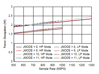
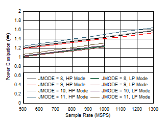
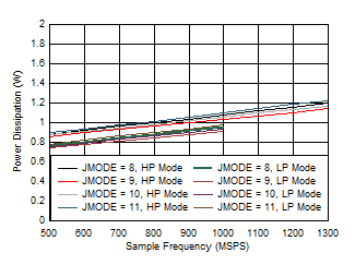
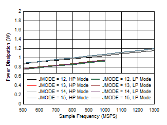
 Figure 5-83 Quad Channel, Power Dissipation vs FS for JMODES 8 -
11
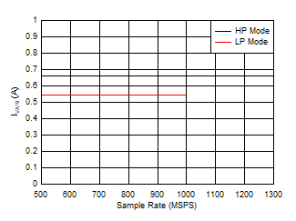
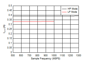
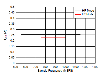
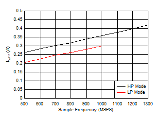
 Figure 5-85 Quad Channel, IVA19 vs FS
| independent of power mode |
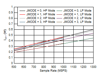
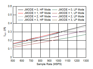
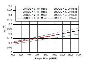
Figure 5-87 Quad
Channel, IVD11 vs FS and JMODE 0 - 3
| independent of power mode |
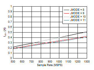
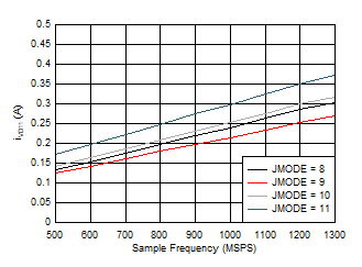
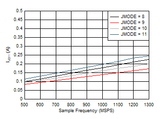
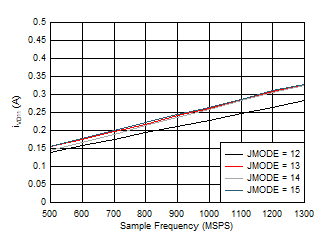
Figure 5-89 Quad Channel, IVD11 vs FS and JMODE 8 -
11 Figure 5-91 Dual Channel, Power Dissipation vs FS for JMODES 0 -
3
 Figure 5-93 Dual Channel, Power Dissipation vs FS for JMODES 8 -
11
 Figure 5-95 Dual Channel, IVA19 vs FS
| independent of power mode |
Figure 5-97 Dual
Channel, IVD11 vs FS and JMODE 0 - 3
| independent of power mode |
Figure 5-99 Dual Channel, IVD11 vs FS and JMODE 8 -
11 Figure 5-101 Single Channel, Power Dissipation vs FS for JMODES 0
- 3
 Figure 5-103 Single Channel, Power Dissipation vs FS for JMODES 8
- 11
 Figure 5-105 Single Channel, IVA19 vs FS
| independent of power mode |
Figure 5-107 Single Channel, IVD11 vs FS and JMODE 0 -
3
| independent of power mode |
Figure 5-109 Single Channel,
IVD11 vs FS and JMODE 8 - 11
| Difference to foreground calibration, JMODE
independent |
Figure 5-111 Quad
Channel, Power Dissipation Change with Calibration Mode
| Difference to foreground calibration, JMODE
independent |
Figure 5-113 Single Channel, Power Dissipation Change with Calibration Mode
| Difference to foreground calibration, JMODE
independent |
Figure 5-115 Dual
Channel, IVA19 Change with Calibration Mode
| Difference to foreground calibration, JMODE
independent |
Figure 5-117 Quad
Channel, IVA11 Change with Calibration Mode
| Difference to foreground calibration, JMODE
independent |
Figure 5-119 Single Channel, IVA11 Change with Calibration Mode
| Difference to foreground calibration, JMODE
independent |
Figure 5-121 Dual
Channel, IVD11 Change with Calibration Mode Figure 5-123 Quad
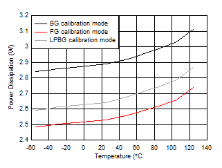
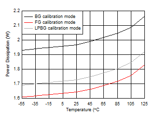
Channel, Power Dissipation vs Temperature
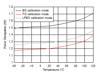
 Figure 5-125 Single Channel, Power Dissipation vs
Temperature
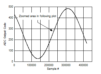
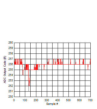
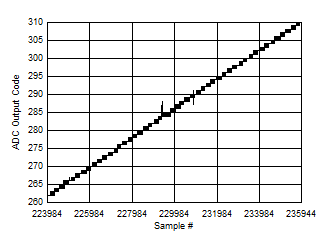
 Figure 5-127 Background Calibration Core Transition (AC Signal)
 Figure 5-129 Background Calibration Core Transition (DC Signal)
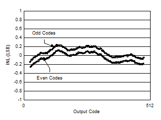
 Figure 5-2 INL
vs Code
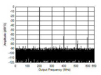
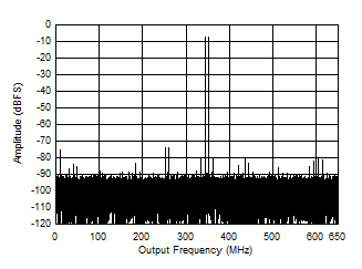
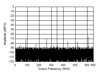
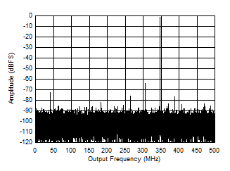
 Figure 5-4 Single Tone FFT at 347 MHz and -1 dBFS
 Figure 5-6 Single Tone FFT at 997 MHz and -1 dBFS
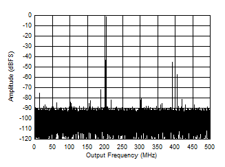
 Figure 5-8 Single Tone FFT at 1797 MHz and -1 dBFS
 Figure 5-10 Single Tone FFT at 3497 MHz and -1 dBFS
| FS = 1000MSPS, Low Power Mode |
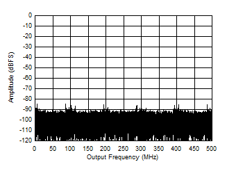
Figure 5-12 Single Tone FFT at 347 MHz and -1 dBFS
| FS = 1000MSPS, Low Power Mode |
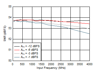
Figure 5-14 Single Tone FFT at 1797 MHz and -1 dBFS Figure 5-16 SNR vs Input Frequency
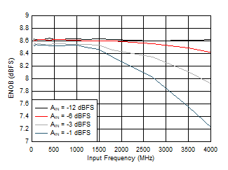
 Figure 5-18 ENOB vs Input Frequency
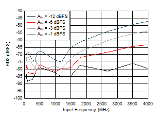
 Figure 5-20 HD3 vs Input Frequency
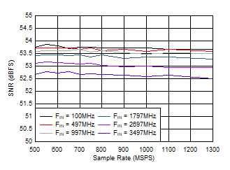
 Figure 5-22 SNR vs Sample Rate
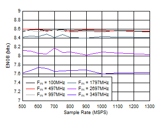
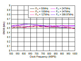
 Figure 5-24 ENOB vs Sample Rate
| FS = 1000MSPS, Low Power Mode |
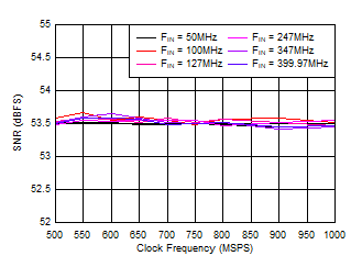
Figure 5-26 SNR vs Sample Rate
| FS = 1000MSPS, Low Power Mode |
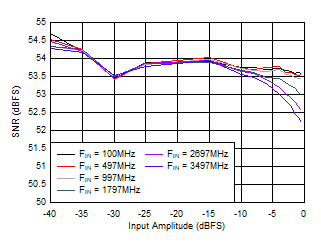
Figure 5-28 ENOB vs Sample Rate Figure 5-30 SNR vs Input Amplitude
| FS = 1000MSPS, FIN = 100MHz,
Low Power Mode |
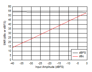
Figure 5-32 SNR
vs Input Amplitude Figure 5-34 SNR
vs Clock Amplitude
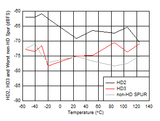
 Figure 5-36 HD2, HD3 and worst non-HD Spur vs
Temperature
| FIN = 997 MHz, FG25°C means calibration
at 25°C and held across temperature |
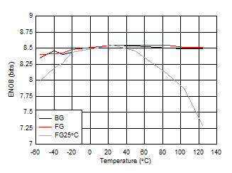
Figure 5-38 ENOB vs Temperature and Calibration Mode
| Low
Power Mode, FIN = 347 MHz, FG25°C means
calibration at 25°C and held across temperature |
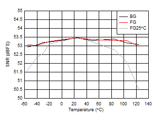
Figure 5-40 SNR vs Temperature and Calibration Mode
| Low
Power Mode, FIN = 347 MHz, FG25°C means
calibration at 25°C and held across temperature |
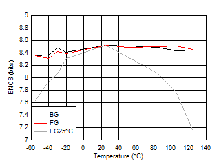
Figure 5-42 ENOB vs Temperature and Calibration Mode Figure 5-44 SNR, SFDR and SINAD vs Supply Voltage
| Low
Power Mode, FIN = 347 MHz, FS =
1000MSPS |
Figure 5-46 SNR, SFDR and SINAD vs Supply Voltage Figure 5-48 Two
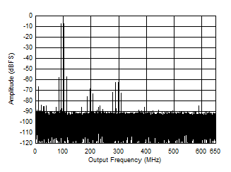
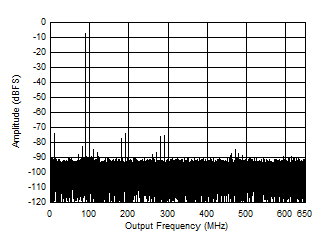
Tone FFT at 95.07 MHz Center
 Figure 5-50 Two
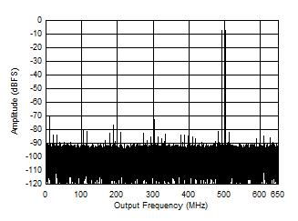
Tone FFT at 498 MHz Center
 Figure 5-52 Two
Tone FFT at 1798 MHz Center
| Low
Power Mode, FS = 1000 MSPS, 10 MHz Tone
Spacing |
Figure 5-54 Two
Tone FFT at 95.07 MHz Center
| Low
Power Mode, FS = 1000 MSPS, 10 MHz Tone
Spacing |
Figure 5-56 Two
Tone FFT at 998 MHz Center
| Low
Power Mode, FS = 1000 MSPS, 10 MHz Tone
Spacing |
Figure 5-58 IMD3 vs Input Frequency  Figure 5-60 Crosstalk to Channel B vs FIN
| FS = 1300MSPS, High Power Mode |
Figure 5-62 SFDR vs Input Frequency and CPLL
| FS = 1300MSPS, High Power Mode |
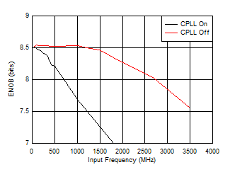
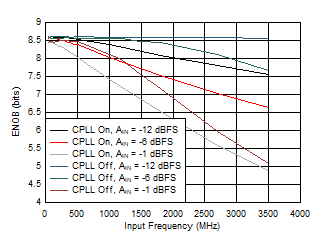
Figure 5-64 ENOB vs Input Frequency and CPLL Figure 5-66 SNR vs Input Frequency and CPLL
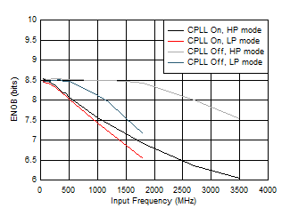
 Figure 5-68 ENOB vs Input Frequency and CPLL
| FS = 1300MSPS, High Power Mode |
Figure 5-70 SFDR vs Input Frequency, CPLL and Input
Amplitude
| FS = 1300MSPS, High Power Mode |
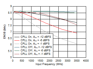
Figure 5-72 ENOB vs Input Frequency, CPLL and Input
Amplitude
| FS = 1300MSPS, High Power Mode |
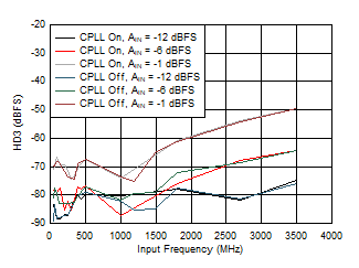
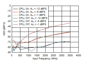
Figure 5-74 HD3 vs Input Frequency, CPLL and Input
Amplitude
| FS = 1000MSPS, Low Power Mode |
Figure 5-76 SFDR vs Input Frequency, CPLL and Input
Amplitude
| FS = 1000MSPS, Low Power Mode |
Figure 5-78 ENOB vs Input Frequency, CPLL and Input
Amplitude
| FS = 1000MSPS, Low Power Mode |
Figure 5-80 HD3 vs Input Frequency, CPLL and Input
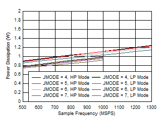
Amplitude Figure 5-82 Quad
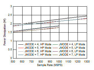
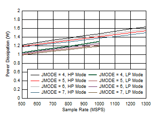
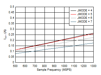
Channel, Power Dissipation vs FS for JMODES 4 - 7
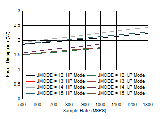
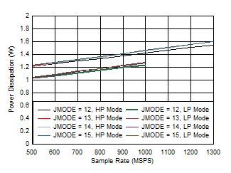
 Figure 5-84 Quad Channel, Power Dissipation vs FS for JMODES 12
- 15
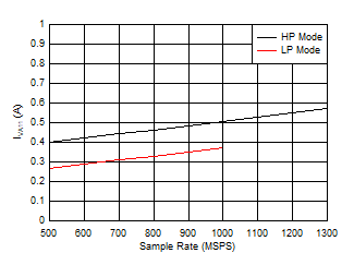
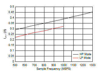
 Figure 5-86 Quad Channel, IVA11 vs FS
| independent of power mode |
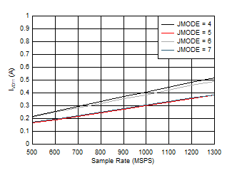
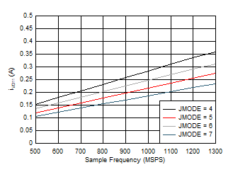
Figure 5-88 Quad Channel, IVD11 vs FS and JMODE 4 -
7
| independent of power mode |
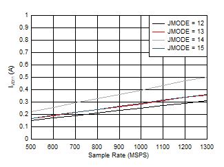
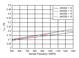
Figure 5-90 Quad Channel, IVD11 vs FS and JMODE 12 -
15 Figure 5-92 Dual Channel, Power Dissipation vs FS for JMODES 4 -
7
 Figure 5-94 Dual Channel, Power Dissipation vs FS for JMODES 12
- 15
 Figure 5-96 Dual Channel, IVA11 vs FS
| independent of power mode |
Figure 5-98 Dual Channel, IVD11 vs FS and JMODE 4 -
7
| independent of power mode |
Figure 5-100 Dual Channel, IVD11 vs FS and JMODE 12 -
15 Figure 5-102 Single Channel, Power Dissipation vs FS for JMODES 4
- 7
 Figure 5-104 Single Channel, Power Dissipation vs FS for JMODES
12 - 15
 Figure 5-106 Single Channel, IVA11 vs FS
| independent of power mode |
Figure 5-108 Single Channel, IVD11 vs FS and JMODE 4 -
7
| independent of power mode |
Figure 5-110 Single Channel, IVD11 vs FS and JMODE 12
- 15
| Difference to foreground calibration, JMODE
independent |
Figure 5-112 Dual
Channel, Power Dissipation Change with Calibration Mode
| Difference to foreground calibration, JMODE
independent |
Figure 5-114 Quad
Channel, IVA19 Change with Calibration Mode
| Difference to foreground calibration, JMODE
independent |
Figure 5-116 Single Channel, IVA19 Change with Calibration Mode
| Difference to foreground calibration, JMODE
independent |
Figure 5-118 Dual
Channel, IVA11 Change with Calibration Mode
| Difference to foreground calibration, JMODE
independent |
Figure 5-120 Quad
Channel, IVD11 Change with Calibration Mode
| Difference to foreground calibration, JMODE
independent |
Figure 5-122 Dual
Channel, IVD11 Change with Calibration Mode Figure 5-124 Dual Channel, Power Dissipation vs
Temperature
 Figure 5-126 Background Calibration Core Transition (midscale voltage)
 Figure 5-128 Background Calibration Core Transition (AC Signal Zoomed)