SNAS466G February 2009 – December 2016 ADC10D1000QML-SP
PRODUCTION DATA.
- 1 Features
- 2 Applications
- 3 Description
- 4 Revision History
- 5 Pin Configuration and Functions
-
6 Specifications
- 6.1 Absolute Maximum Ratings
- 6.2 ESD Ratings
- 6.3 Recommended Operating Conditions
- 6.4 Thermal Information
- 6.5 Converter Electrical Characteristics: Static Converter Characteristics
- 6.6 Converter Electrical Characteristics: Dynamic Converter Characteristics
- 6.7 Converter Electrical Characteristics: Analog Input/Output and Reference Characteristics
- 6.8 Converter Electrical Characteristics: Channel-to-Channel Characteristics
- 6.9 Converter Electrical Characteristics: LVDS CLK Input Characteristics
- 6.10 Electrical Characteristics: AutoSync Feature
- 6.11 Converter Electrical Characteristics: Digital Control and Output Pin Characteristics
- 6.12 Converter Electrical Characteristics: Power Supply Characteristics (1:2 Demux Mode)
- 6.13 Converter Electrical Characteristics: AC Electrical Characteristics
- 6.14 Timing Requirements: Serial Port Interface
- 6.15 Timing Requirements: Calibration
- 6.16 Quality Conformance Inspection
- 6.17 Timing Diagrams
- 6.18 Typical Characteristics
-
7 Detailed Description
- 7.1 Overview
- 7.2 Functional Block Diagram
- 7.3 Feature Description
- 7.4
Device Functional Modes
- 7.4.1
Control Modes
- 7.4.1.1
Non-Extended Control Mode
- 7.4.1.1.1 Non-Demultiplexed Mode Pin (NDM)
- 7.4.1.1.2 Dual Data-Rate Phase Pin (DDRPh)
- 7.4.1.1.3 Calibration Pin (CAL)
- 7.4.1.1.4 Power-Down I-Channel Pin (PDI)
- 7.4.1.1.5 Power-Down Q-Channel Pin (PDQ)
- 7.4.1.1.6 Test Pattern Mode Pin (TPM)
- 7.4.1.1.7 Full-Scale Input Range Pin (FSR)
- 7.4.1.1.8 AC-DC-Coupled Mode Pin (VCMO)
- 7.4.1.1.9 LVDS Output Common-Mode Pin (VBG)
- 7.4.1.1
Non-Extended Control Mode
- 7.4.2 Extended Control Mode
- 7.4.1
Control Modes
- 7.5 Programming
- 7.6 Register Maps
- 8 Application and Implementation
- 9 Power Supply Recommendations
- 10Layout
- 11Device and Documentation Support
- 12Mechanical, Packaging, and Orderable Information
8 Application and Implementation
NOTE
Information in the following applications sections is not part of the TI component specification, and TI does not warrant its accuracy or completeness. TI’s customers are responsible for determining suitability of components for their purposes. Customers should validate and test their design implementation to confirm system functionality.
8.1 Application Information
8.1.1 Analog Inputs
The ADC10D1000 continuously converts any signal which is present at the analog inputs, as long as a CLK signal is also provided to the device. This section covers important aspects related to the analog inputs including: acquiring the input, the reference voltage and FSR, out-of-range indication, AC-coupled signals, and single-ended input signals.
8.1.1.1 Acquiring the Input
Data is acquired at the rising edge of CLK+ in non-DES mode and both the falling and rising edge of CLK+ in DES mode. The digital equivalent of that data is available at the digital outputs a constant number of input clock cycles later for the DI, DQ, DId and DQd output buses, also known as latency, depending on the demultiplex mode which was chosen. See tLAT in Converter Electrical Characteristics: AC Electrical Characteristics. In addition to latency, there is a constant output delay, tOD, before the data is available at the outputs. See tOD in Converter Electrical Characteristics: AC Electrical Characteristics and Timing Diagrams.
For demux mode, the signal which is sampled at the input will appear at the output after a certain latency, as shown in Table 27.
Table 27. Input Channel Samples Produced at Data Outputs in Demultiplexed Mode
| DATA OUTPUTS | NON-DES MODE | DES MODE (Q channel ONLY) |
|---|---|---|
| DI | I channel sampled with rise of CLK, 34 cycles earlier. |
Q channel sampled with rise of CLK, 34 cycles earlier. |
| DQ | Q channel sampled with rise of CLK, 34 cycles earlier. |
Q channel sampled with fall of CLK, 34.5 cycles earlier. |
| DId | I channel sampled with rise of CLK, 35 cycles earlier. |
Q channel sampled with rise of CLK, 35 cycles earlier. |
| DQd | Q channel sampled with rise of CLK, 35 cycles earlier. |
Q channel sampled with fall of CLK, 35.5 cycles earlier. |
Non-Demux Mode is similarly shown in Table 28.
Table 28. Input Channel Samples Produced at Data Outputs in Non-Demux Mode
| DATA OUTPUTS | NON-DES MODE | DES MODE (Q channel ONLY) |
|---|---|---|
| DI | I channel sampled with rise of CLK, 34 cycles earlier. |
Q channel sampled with rise of CLK, 34 cycles earlier. |
| DQ | Q channel sampled with rise of CLK, 34 cycles earlier. |
Q channel sampled with fall of CLK, 34.5 cycles earlier. |
| DId | No output; high impedance. |
No output; high impedance. |
| DQd | No output; high impedance. |
No output; high impedance. |
8.1.1.2 Terminating Unused Analog Inputs
In the case that only one channel is used in non-des mode or that the ADC is driven in DESI or DESQ mode, the unused analog input must be terminated to reduce any noise coupling into the ADC. See Table 29 for details.
Table 29. Unused Analog Input Recommended Termination
| MODE | POWER DOWN | COUPLING | RECOMMENDED TERMINATION |
|---|---|---|---|
| Non-DES | Yes | AC/DC | Tie unused+ and unused– to VBG |
| DES/ Non-DES | No | DC | Tie unused+ and unused– to VBG |
| DES/ Non-DES | No | AC | Tie unused+ to unused– |
8.1.1.3 Reference Voltage and FSR
The full-scale analog differential input range (VIN_FSR) of the ADC10D1000 is derived from an internal 1.254-V bandgap reference. In non-ECM, this full-scale range has two settings controlled by the FSR pin; see Full-Scale Input Range Pin (FSR). The FSR pin operates on both the I channel and the Q channel. In ECM, the full-scale range may be independently set for each channel via the I-channel and Q-channel Full-Scale Range Adjust Registers (Addr: 3h and Bh, respectively) with 15 bits of precision; see Register Maps. The best SNR is obtained with a higher full-scale input range, but better distortion and SFDR are obtained with a lower full-scale input range. It is not possible to use an external analog reference voltage to modify the full-scale range, and this adjustment should only be done digitally, as described.
A buffered version of the internal 1.254-V bandgap reference voltage is made available at the VBG pin for the user. The VBG pin can drive a load of up to 80 pF and source or sink up to ±100 μA; it must be buffered if more current than this is required. The pin remains as a constant reference voltage regardless of what full-scale range is selected and may be used for a system reference. VBG is a dual-purpose pin and it may also be used to select a higher LVDS output common-mode voltage; see LVDS Output Common-Mode Voltage.
8.1.1.4 Out-of-Range Indication
Differential input signals are digitized to 10 bits, based on the full-scale range. Signal excursions beyond the full-scale range (greater than +VIN / 2 or less than –VIN / 2) are clipped at the output. An input signal that is above the FSR results in all 1's at the output and an input signal which is below the FSR results in all 0's at the output. When the conversion result is clipped for the I-channel input, the ORI I-channel output is activated such that ORI+ goes high and ORI– goes low for the time that the signal is out of range. This output is active as long as accurate data on either or both of the buses would be outside the range of 000h to 3FFh. The Q channel has a separate ORQ which functions similarly.
8.1.1.5 AC-Coupled Input Signals
The ADC10D1000QML-SP analog inputs require a precise common-mode voltage. This voltage is generated onchip when AC-coupling mode is selected. See AC-DC-Coupled Mode Pin (VCMO) for more information about how to select AC-coupled mode.
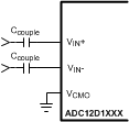
In AC-coupled mode, the analog inputs must of course be AC-coupled. For an ADC10D1000QML-SP used in a typical application, this may be accomplished by on-board capacitors, as shown in Figure 44.
When the AC-coupled mode is selected, an analog input channel that is not used (for example, in DES mode) must be connected to AC ground — for example, through capacitors to ground. Do not connect an unused analog input directly to ground.
 Figure 44. AC-Coupled Differential Input
The analog inputs for the ADC10D1000QML-SP are internally buffered, which simplifies the task of driving these inputs and the RC pole, which is generally used at sampling ADC inputs, is not required. If the user desires to place an amplifier circuit before the ADC, take care to choose an amplifier with adequate noise and distortion performance, and adequate gain at the frequencies used for the application.
8.1.1.6 DC-Coupled Input Signals
In DC-coupled mode, the ADC10D1000QML-SP differential inputs must have the correct common-mode voltage. This voltage is provided by the device itself at the VCMO output pin. TI recommends using this voltage because the VCMO output potential changes with temperature and the common-mode voltage of the driving device must track this change. Full-scale distortion performance falls off as the input common-mode voltage deviates from VCMO. Therefore, TI recommends keeping the input common-mode voltage within 100 mV of VCMO (typical), although this range may be extended to ±150 mV (maximum).
8.1.1.7 Single-Ended Input Signals
It is not possible on the ADC10D1000 to accept single-ended signals. The best way to handle single-ended signals is to first convert them to differential signals before presenting them to the ADC. The easiest way to accomplish single-ended to differential signal conversion is with an appropriate balun-transformer, as shown in Figure 45.
 Figure 45. Single-Ended-to-Differential Conversion Using a Balun
When selecting a balun, it is important to understand the input architecture of the ADC. The impedance of the analog source must be matched to the ADC10D1000's on-chip 100-Ω differential input termination resistor. The range of this termination resistor is specified as RIN in Converter Electrical Characteristics: Analog Input/Output and Reference Characteristics.
8.1.2 Clock Inputs
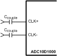
The ADC10D1000 has a differential clock input, CLK+ and CLK–, which must be driven with an AC-coupled, differential clock signal. This provides the level shifting to the clock to be driven with LVDS, PECL, LVPECL, or CML levels. The clock inputs are internally terminated to 100-Ω differential and self-biased. This section covers coupling, frequency range, level, duty-cycle, jitter, and layout considerations.
8.1.2.1 CLK Coupling
The clock inputs of the ADC10D1000 must be capacitively coupled to the clock pins as indicated in Figure 46.
 Figure 46. Differential Input Clock Connection
The choice of capacitor values depends on the clock frequency, capacitor component characteristics, and other system factors.
8.1.2.2 CLK Frequency
Although the ADC10D1000 is tested and its performance is ensured with a differential 1-GHz clock, the device typically functions well over the input clock frequency range; see fCLK (min) and fCLK (max) in Converter Electrical Characteristics: AC Electrical Characteristics. Operation up to fCLK (max) is possible if the maximum ambient temperatures indicated are not exceeded. Operating at sample rates above fCLK (max) for the maximum ambient temperature may result in reduced device reliability and product lifetime. This is due to the fact that higher sample rates results in higher power consumption and die temperatures. If the fCLK ≤ 300 MHz, enable LFS in control register (Addr: 0h Bit 8).
8.1.2.3 CLK Level
The input clock amplitude is specified as VIN_CLK in Converter Electrical Characteristics: LVDS CLK Input Characteristics. Input clock amplitudes above the maximum VIN_CLK may result in increased input offset voltage. This would cause the converter to produce an output code other than the expected 511/512 when both input pins are at the same potential. Insufficient input clock levels will result in poor dynamic performance. Both of these results may be avoided by keeping the clock input amplitude within the specified limits of VIN_CLK.
8.1.2.4 CLK Duty Cycle
The duty cycle of the input clock signal can affect the performance of any ADC. The ADC10D1000 features a duty-cycle-clock correction circuit, which can maintain performance over the 20%-to-80% specified clock duty cycle range. This feature is enabled by default and provides improved ADC clocking, especially in the dual-edge sampling (DES) mode.
8.1.2.5 CLK Jitter
High-speed, high-performance ADCs such as the ADC10D1000 require a very stable input clock signal with minimum phase noise or jitter. ADC jitter requirements are defined by the ADC resolution (number of bits), maximum ADC input frequency and the input signal amplitude relative to the ADC input full-scale range. The maximum jitter (the sum of the jitter from all sources) allowed to prevent a jitter-induced reduction in SNR is found to be
where
- tJ(MAX) is the rms total of all jitter sources in seconds
- VIN(P-P) is the peak-to-peak analog input signal
- VFSR is the full-scale range of the ADC
- N is the ADC resolution in bits
- fIN is the maximum input frequency, in Hertz, at the ADC analog input
tJ(MAX) is the square root of the sum of the squares (RSS) sum of the jitter from all sources, including the ADC input clock, system, input signals and the ADC itself. Since the effective jitter added by the ADC is beyond user control, TI recommends keeping the sum of all other externally added jitter to a mimimum.
8.1.2.6 CLK Layout
The ADC10D1000 clock input is internally terminated with a trimmed 100-Ω resistor. The differential input clock line pair must have a characteristic impedance of 100 Ω and (when using a balun), be terminated at the clock source in that (100-Ω) characteristic impedance.
It is good practice to keep the ADC input clock line as short as possible, to keep it well away from any other signals, and to treat it as a transmission line. Otherwise, other signals can introduce jitter into the input clock signal. Also, the clock signal can also introduce noise into the analog path if it is not properly isolated.
8.1.3 The LVDS Outputs
The Data, ORI, ORQ, DCLKI, and DCLKQ outputs are LVDS. The electrical specifications of the LVDS outputs are compatible with typical LVDS receivers available on ASIC and FPGA chips, but they are not IEEE or ANSI communications standards compliant due to the low 1.9-V supply used on this device. These outputs must be terminated with a 100-Ω differential resister placed as closely as possible to the receiver. This section covers common-mode and differential voltage, and data rate.
8.1.3.1 Common-Mode and Differential Voltage
The LVDS outputs have selectable common-mode and differential voltage, VOS and VOD; see Converter Electrical Characteristics: Digital Control and Output Pin Characteristics. See Output Control and Adjust for more information.
Selecting the higher VOS also increases VOD by up to 40 mV. The differential voltage, VOD, may be selected for the higher or lower value. For short LVDS lines and low noise systems, satisfactory performance may be realized with the lower VOD. This also results in lower power consumption. If the LVDS lines are long and/or the system in which the ADC10D1000 is used is noisy, it may be necessary to select the higher VOD.
8.1.3.2 Output Data Rate
The data is produced at the output at the same rate as it is sampled at the input. The minimum recommended input clock rate for this device is fCLK (MIN); see Converter Electrical Characteristics: AC Electrical Characteristics. However, it is possible to operate the device in 1:2 demux mode and capture data from just one 10-bit bus, for example, just DI (or DId) although both DI and DId are fully operational. This will decimate the data by two and effectively halve the data rate.
8.1.4 Synchronizing Multiple ADC10D1000S in a System
The ADC10D1000 has two features to assist the user with synchronizing multiple ADCs in a system: AutoSync and DCLK Reset. The AutoSync feature is new and designates one ADC10D1000 as the master ADC and other ADC10D1000s in the system as Slave ADCs. The DCLK Reset feature performs the same function as the AutoSync feature, but is the first generation solution to synchronizing multiple ADCs in a system; it is disabled by default. For applications in which there are multiple master and slave ADC10D1000s in a system, AutoSync may be used to synchronize the slave ADC10D1000(s) to each respective master ADC10D1000, and the DCLK Reset may be used to synchronize the master ADC10D1000s with each other.
If the AutoSync or DCLK reset feature is not used, see Table 30 for recommendations about terminating unused ins.
Table 30. Unused AutoSync and DCLK Pin Recommendations
| PIN(s) | UNUSED TERMINATION |
|---|---|
| RCLK+, RCLK– | Do not connect. |
| RCOUT1+, RCOUT– | Do not connect. |
| RCOUT2+, RCOUT– | Do not connect. |
| DCLK_RST+ | Connect to GND with a 1-kΩ resistor. |
| DCLK_RST– | Connect to VA with a 1-kΩ resistor. |
8.1.4.1 AutoSync Feature
AutoSync is a new feature, which continuously synchronizes the outputs of multiple ADC10D1000s in a system. It may be used to synchronize the DCLK and data outputs of one or more dlave ADC10D1000s to one master ADC10D1000. Several advantages of this feature include no special synchronization pulse required, any upset in synchronization is recovered upon the next DCLK cycle, and the master/dlave ADC10D1000s may be arranged as a binary tree so that any upset quickly propagates out of the system.
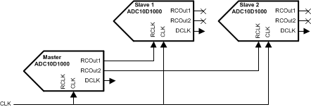
An example system, which consists of one master ADC and two slave ADCs, is shown in Figure 47. For simplicity, only one DCLK is shown; in reality, there is DCLKI and DCLKQ, but they are always in phase with one another.
 Figure 47. AutoSync Example
In order to synchronize the DCLK (and data) outputs of multiple ADCs, the DCLKs must transition at the same time, as well as be in phase with one another. The DCLK at each ADC is generated from the CLK after some latency, plus tOD minus tAD. Therefore, in order for the DCLKs to transition at the same time, the CLK signal must reach each ADC at the same time. To tune out any differences in the CLK path to each ADC, the tAD adjust feature may be used. However, using the tAD adjust feature will also affect when the DCLK is produced at the output. If the device is in demux mode, then there are four possible phases which each DCLK may be generated on because the typical CLK = 1 GHz and DCLK = 250 MHz for this case. The RCLK signal controls the phase of the DCLK, so that each Slave DCLK is on the same phase as the Master DCLK.
The AutoSync feature may only be used via the Control Registers. For more information, see AN-2132 Synchronizing Multiple GSPS ADCs in a System: The AutoSync Feature (SNAA073).
8.1.4.2 DCLK Reset Feature
The DCLK reset feature is available via ECM, but is disabled by default. DCLKI and DCLKQ are always synchronized, by design, and do not require a pulse from DCLK_RST to become synchronized.
The DCLK_RST signal must observe certain timing requirements, which are shown in Figure 5 of Timing Diagrams. The DCLK_RST pulse must be of a minimum width and its deassertion edge must observe setup and hold times with respect to the CLK input rising edge. These timing specifications are listed as tPWR, tSR and tHR and may be found in Converter Electrical Characteristics: AC Electrical Characteristics.
The DCLK_RST signal can be asserted asynchronously to the input clock. If DCLK_RST is asserted, the DCLK output is held in a designated state (logic-high) in demux mode; in non-demux mode, the DCLK continues to function normally. Depending upon when the DCLK_RST signal is asserted, there may be a narrow pulse on the DCLK line during this reset event When the DCLK_RST signal is de-asserted, there are tSYNC_DLY CLK cycles of systematic delay, and the next CLK rising edge synchronizes the DCLK output with those of other ADC10D1000s in the system. For 90° mode (DDRPh = logic-high), the synchronizing edge occurs on the rising edge of CLK, 4 cycles after the first rising edge of CLK after DCLK_RST is released. For 0° mode (DDRPh = logic-low), this is 5 cycles instead. The DCLK output is enabled again after a constant delay of tOD.
For both demux and non-demux modes, there is some uncertainty about how DCLK comes out of the reset state for the first DCLK_RST pulse. For the second (and subsequent) DCLK_RST pulses, the DCLK comes out of the reset state in a known way. Therefore, if using the DCLK reset feature, TI recommends applying one dummy DCLK_RST pulse before using the second DCLK_RST pulse to synchronize the outputs. This recommendation applies each time the device or channel is powered on.
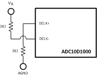
When the DCLK_RST function is not going to be used TI recommends pulling the DCLK+ pin to GND through a 261-Ω resister and pulling the DCLK− pin to VA through a 261-Ω resistor (see Figure 48). This provides noise immunity and prevent false resets.
 Figure 48. DCLK RST±
When using DCLK-RST to synchronize multiple ADC10D1000s, it is required that the select phase bits in the Control Register (Addr: Eh, Bits 3,4) be the same for each Slave ADC10D1000.