SNAS483F February 2010 – August 2015 ADC128D818
PRODUCTION DATA.
- 1 Features
- 2 Applications
- 3 Description
- 4 Revision History
- 5 Description (continued)
- 6 Pin Configuration and Functions
- 7 Specifications
-
8 Detailed Description
- 8.1 Overview
- 8.2 Functional Block Diagram
- 8.3 Feature Description
- 8.4 Device Functional Modes
- 8.5 Programming
- 8.6
Register Maps
- 8.6.1 ADC128D818 Internal Registers
- 8.6.2 Configuration Register — Address 00h
- 8.6.3 Interrupt Status Register — Address 01h
- 8.6.4 Interrupt Mask Register — Address 03h
- 8.6.5 Conversion Rate Register — Address 07h
- 8.6.6 Channel Disable Register — Address 08h
- 8.6.7 One-Shot Register — Address 09h
- 8.6.8 Deep Shutdown Register — Address 0Ah
- 8.6.9 Advanced Configuration Register — Address 0Bh
- 8.6.10 Busy Status Register — Address 0Ch
- 8.6.11 Channel Readings Registers — Addresses 20h - 27h
- 8.6.12 Limit Registers — Addresses 2Ah - 39h
- 8.6.13 Manufacturer ID Register — Address 3Eh
- 8.6.14 Revision ID Register — Addresses 3Fh
-
9 Application and Implementation
- 9.1 Application Information
- 9.2
Typical Application
- 9.2.1 Design Requirements
- 9.2.2
Detailed Design Procedure
- 9.2.2.1 Power Management
- 9.2.2.2
Using the ADC128D818
- 9.2.2.2.1 Quick Start
- 9.2.2.2.2 Poweron Reset (POR)
- 9.2.2.2.3 Configuration Register (address 00h)
- 9.2.2.2.4 Interrupt Status Register (address 01h)
- 9.2.2.2.5 Interrupt Mask Register (address 03h)
- 9.2.2.2.6 Conversion Rate Register (address 07h)
- 9.2.2.2.7 One-Shot Register (address 09h)
- 9.2.2.2.8 Deep Shutdown Register (address 0Ah)
- 9.2.2.2.9 Channel Readings Registers (addresses 20h - 27h)
- 9.2.3 Application Curve
- 9.3 System Examples
- 10Power Supply Recommendations
- 11Layout
- 12Device and Documentation Support
- 13Mechanical, Packaging, and Orderable Information
11 Layout
11.1 Layout Guidelines
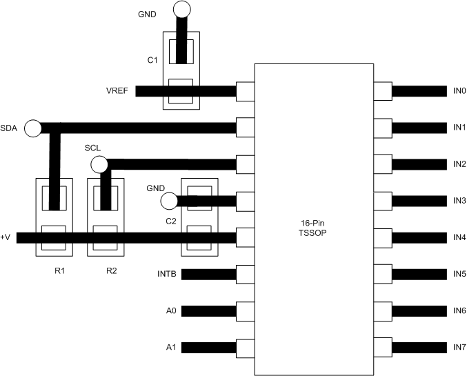
Analog inputs will provide best accuracy when referred to the GND pin or a supply with low noise. A separate, low-impedance ground plane for analog ground, which provides a ground point for the voltage dividers and analog components, will provide best performance but is not mandatory. Analog components such as voltage dividers must be located physically as close as possible to the ADC128D818.
11.2 Layout Example
 Figure 42. Sample Layout