SNAS483F February 2010 – August 2015 ADC128D818
PRODUCTION DATA.
- 1 Features
- 2 Applications
- 3 Description
- 4 Revision History
- 5 Description (continued)
- 6 Pin Configuration and Functions
- 7 Specifications
-
8 Detailed Description
- 8.1 Overview
- 8.2 Functional Block Diagram
- 8.3 Feature Description
- 8.4 Device Functional Modes
- 8.5 Programming
- 8.6
Register Maps
- 8.6.1 ADC128D818 Internal Registers
- 8.6.2 Configuration Register — Address 00h
- 8.6.3 Interrupt Status Register — Address 01h
- 8.6.4 Interrupt Mask Register — Address 03h
- 8.6.5 Conversion Rate Register — Address 07h
- 8.6.6 Channel Disable Register — Address 08h
- 8.6.7 One-Shot Register — Address 09h
- 8.6.8 Deep Shutdown Register — Address 0Ah
- 8.6.9 Advanced Configuration Register — Address 0Bh
- 8.6.10 Busy Status Register — Address 0Ch
- 8.6.11 Channel Readings Registers — Addresses 20h - 27h
- 8.6.12 Limit Registers — Addresses 2Ah - 39h
- 8.6.13 Manufacturer ID Register — Address 3Eh
- 8.6.14 Revision ID Register — Addresses 3Fh
-
9 Application and Implementation
- 9.1 Application Information
- 9.2
Typical Application
- 9.2.1 Design Requirements
- 9.2.2
Detailed Design Procedure
- 9.2.2.1 Power Management
- 9.2.2.2
Using the ADC128D818
- 9.2.2.2.1 Quick Start
- 9.2.2.2.2 Poweron Reset (POR)
- 9.2.2.2.3 Configuration Register (address 00h)
- 9.2.2.2.4 Interrupt Status Register (address 01h)
- 9.2.2.2.5 Interrupt Mask Register (address 03h)
- 9.2.2.2.6 Conversion Rate Register (address 07h)
- 9.2.2.2.7 One-Shot Register (address 09h)
- 9.2.2.2.8 Deep Shutdown Register (address 0Ah)
- 9.2.2.2.9 Channel Readings Registers (addresses 20h - 27h)
- 9.2.3 Application Curve
- 9.3 System Examples
- 10Power Supply Recommendations
- 11Layout
- 12Device and Documentation Support
- 13Mechanical, Packaging, and Orderable Information
7 Specifications
7.1 Absolute Maximum Ratings
over operating free-air temperature range (unless otherwise noted)(6)(3)(1)Æ(2)| MIN | MAX | UNIT | ||
|---|---|---|---|---|
| Supply Voltage (V+) | 6.0 | 6 | V | |
| Voltage on SCL, SDA, A0, A1, INT | –0.3 | 6 | V | |
| Voltage on IN0-IN7, VREF | –0.3 | (V+ + 0.3) | V | |
| Input Current at Any Pin(4) | ±5 | mA | ||
| Package Input Current(4) | ±30 | mA | ||
| Maximum Junction Temperature (TJMAX)(5) | 150 | °C | ||
| Storage Temperature, Tstg | –65 | 150 | °C | |
(1) Stresses beyond those listed under Absolute Maximum Ratings may cause permanent damage to the device. These are stress ratings only, which do not imply functional operation of the device at these or any other conditions beyond those indicated under Recommended Operating Conditions. Exposure to absolute-maximum-rated conditions for extended periods may affect device reliability.
(2) For soldering specifications, SNOA549
(3) If Military/Aerospace specified devices are required, please contact the Texas Instruments Sales Office/Distributors for availability and specifications.
(4) If the input voltage at any pin exceeds the power supply ( that is, VIN < GND or VIN > V +) but is less than the absolute maximum ratings, then the current at that pin must be limited to 5 mA. The 30 mA maximum package input current rating limits the number of pins that can safely exceed the power supply with an input current of 5 mA to six pins. Parasitic components and/or ESD protection circuitry are shown in the Pin Descriptions table.
(5) The maximum power dissipation must be derated at elevated temperatures and is dictated by TJMAX, RθJA and the ambient temperature, TA. The maximum allowable power dissipation at any temperature is PD = (TJMAX − T A) / RθJA.
(6) All voltages are measured with respect to GND, unless otherwise specified.
7.2 ESD Ratings
| VALUE | UNIT | |||
|---|---|---|---|---|
| V(ESD) | Electrostatic discharge | Human body model (HBM), per ANSI/ESDA/JEDEC JS-001(1) | ±3000 | V |
| Charged-device model (CDM), per JEDEC specification JESD22-C101(2) | ±1000 | |||
| Machine model | ±300 | |||
(1) JEDEC document JEP155 states that 500-V HBM allows safe manufacturing with a standard ESD control process.
(2) JEDEC document JEP157 states that 250-V CDM allows safe manufacturing with a standard ESD control process.
7.3 Recommended Operating Conditions
over operating free-air temperature range (unless otherwise noted(1)| MIN | MAX | UNIT | ||
|---|---|---|---|---|
| Supply Voltage (V+) | 3 | 5.5 | V | |
| Voltage on SCL, SDA, A0, A1, INT | –0.05 | 5.5 | V | |
| Voltage on IN0-IN7, VREF | –0.05 | (V+ + 0.05) | V | |
| Temperature Range for Electrical Characteristics | –40 | 125 | °C | |
| Operating Temperature | –40 | 125 | °C | |
(1) All voltages are measured with respect to GND, unless otherwise specified.
7.4 Thermal Information
| THERMAL METRIC(1) | ADC128D818 | UNIT | |
|---|---|---|---|
| PW (TSSOP) | |||
| 16 PINS | |||
| RθJA | Junction-to-ambient thermal resistance | 130 | °C/W |
(1) For more information about traditional and new thermal metrics, see the Semiconductor and IC Package Thermal Metrics application report, SPRA953.
7.5 DC Electrical Characteristics
The following specifications apply for 3 VDC ≤ V+ ≤ 5.5 VDC , External VREF = 2.56 V, unless otherwise specified. All limits TA = TJ = 25°C unless otherwise specified(7).| PARAMETER | TEST CONDITIONS | MIN(6) | TYP(5) | MAX(6) | UNIT | |||
|---|---|---|---|---|---|---|---|---|
| POWER SUPPLY CHARACTERISTICS | ||||||||
| V+ | Supply Voltage | 3.3 or 5 | V | |||||
| TA = TJ = TMIN to TMAX | 3 | 5.5 | ||||||
| VREF | External Reference Voltage | 2.56 | V | |||||
| TA = TJ = TMIN to TMAX | 1.25 | V+ | ||||||
| Internal Reference Voltage | 2.56 | V | ||||||
| 23 | ppm/°C | |||||||
| I+ | Supply Current (see Power Management). | Interface Inactive, V+ = 5.5 V, Mode 2 | TA = TJ = TMIN to TMAX | 0.74 | mA | |||
| Interface Inactive, V+ = 3.6 V, Mode 2 | TA = TJ = TMIN to TMAX | 0.56 | mA | |||||
| Shutdown Mode, V+ = 5.5 V | TA = TJ = TMIN to TMAX | 0.65 | mA | |||||
| Shutdown Mode, V+ = 3.6 V | TA = TJ = TMIN to TMAX | 0.48 | mA | |||||
| Deep Shutdown Mode(1). | TA = TJ = TMIN to TMAX | 10 | µA | |||||
| TEMPERATURE-to-DIGITAL CONVERTER CHARACTERISTICS | ||||||||
| Temperature Error | –40°C ≤ TA ≤ +125°C | TA = TJ = TMIN to TMAX | ±3 | °C | ||||
| –25°C ≤ TA ≤ +100°C | TA = TJ = TMIN to TMAX | ±2 | °C | |||||
| Resolution | 0.5 | °C | ||||||
| ANALOG-to-DIGITAL CONVERTER CHARACTERISTICS | ||||||||
| n | Resolution | 12-bit with full-scale at VREF = 2.56 V. | 0.625 | mV | ||||
| INL | Integral Non-Linearity | External VREF = 1.25 V, Pseudo-Differential, V+ = 3 V to 3.3 V.(1) | 0.36 | LSb | ||||
| TA = TJ = TMIN to TMAX | –1 | 1 | ||||||
| External VREF = 2.56 V, Pseudo-Differential | 1.58 | LSb | ||||||
| TA = TJ = TMIN to TMAX | –2 | 4 | ||||||
| External VREF = 5 V, Pseudo-Differential, V+ = 5 V to 5.5 V. | ||||||||
| DNL | Differential Non-Linearity | See (2) | ±0.25 | LSb | ||||
| TA = TJ = TMIN to TMAX | –1 | 1 | ||||||
| TUE | Total Unadjusted Error(3) | Internal VREF, Single-Ended, V+ = 3 V to 3.6 V. | TA = TJ = TMIN to TMAX | –0.5 | 0.5 | % of FS | ||
| Internal VREF, Single-Ended, V+ = 4.5 V to 5.5 V(4). | ||||||||
| Internal VREF, Pseudo-Differential, V+ = 3 V to 3.6 V or V+ = 4.5 V to 5.5 V(4). | TA = TJ = TMIN to TMAX | –0.3 | 0.5 | % of FS | ||||
| External VREF = 1.25 V, Single-Ended, V+ = 3 V to 3.6 V. | TA = TJ = TMIN to TMAX | –0.6 | 0.1 | % of FS | ||||
| External VREF = 2.56 V, Single-Ended, V+ = 3 V to 5.5 V. | TA = TJ = TMIN to TMAX | |||||||
| External VREF = 1.25 V, Pseudo-Differential, V+ = 3 V to 3.6 V. | TA = TJ = TMIN to TMAX | –0.45 | 0.2 | % of FS | ||||
| External VREF = 2.56 V, Pseudo-Differential, V+ = 3 V to 5.5 V. | TA = TJ = TMIN to TMAX | |||||||
| GE | Gain Error | Internal VREF, V+ = 3 V to 3.6 V. | TA = TJ = TMIN to TMAX | –0.25 | 0.45 | % of FS | ||
| Internal VREF, V+ = 4.5 V to 5.5 V(4) | ||||||||
| External VREF = 1.25 V or 2.56 V, V+ = 3 V to 3.6 V. | TA = TJ = TMIN to TMAX | –0.45 | 0.2 | % of FS | ||||
| External VREF = 2.56 V or 5 V, V+ = 4.5 V to 5.5 V. | ||||||||
| OE | Offset Error | Internal VREF, Pseudo-Differential,V+ = 4.5 V to 5.5 V(4). | TA = TJ = TMIN to TMAX | –0.15 | 0.2 | % of FS | ||
| External VREF = 1.25 V or 2.56 V, Single-Ended, V+ = 3 V to 3.6 V. | TA = TJ = TMIN to TMAX | –0.5 | 0.1 | % of FS | ||||
| External VREF = 2.56 V or 5 V, Single-Ended, V+ = 4.5 V to 5.5 V | ||||||||
| External VREF = 1.25 V or 2.56 V, Pseudo-Differential, V+ = 3 V to 3.6 V. | TA = TJ = TMIN to TMAX | –0.2 | 0.15 | % of FS | ||||
| External VREF = 2.56 V or 5 V, Pseudo-Differential, V+ = 4.5 V to 5.5 V | ||||||||
| tC | Continuous Conversion Mode | Each Enabled Voltage Channel | 12 | ms | ||||
| Internal Temperature Sensor | 3.6 | ms | ||||||
| Low Power Conversion Mode | Enabled Voltage Channel(s) and Internal Temperature Sensor | 728 | ms | |||||
| MULTIPLEXER / ADC INPUT CHARACTERISTICS | ||||||||
| RON | ON-Resistance | 2 | kΩ | |||||
| TA = TJ = TMIN to TMAX | 10 | |||||||
| ION | Input Current (On Channel Leakage Current) | ±0.005 | μA | |||||
| IOFF | Off Channel Leakage Current | ±0.005 | μA | |||||
| DIGITAL OUTPUTS: INT | ||||||||
| VOUT(0) | Logical 0 Output Voltage | IOUT = 5.0 mA at V+ = 4.5 V, IOUT = +3 mA at V+ = +3 V | TA = TJ = TMIN to TMAX | 0.4 | V | |||
| OPEN DRAIN SERIAL BUS OUTPUT: SDA | ||||||||
| VOUT(0) | Logical 0 Output Voltage | IOUT = 3.0 mA at V+ = 4.5 V, | TA = TJ = TMIN to TMAX | 0.4 | V | |||
| IOH | High Level Output Current | VOUT = V+ | 0.005 | μA | ||||
| TA = TJ = TMIN to TMAX | 1 | |||||||
| DIGITAL INPUTS: A0 and A1 | ||||||||
| VIN(1) | Logical 1 Input Voltage | TA = TJ = TMIN to TMAX | 0.9 × V+ | 5.5 | V | |||
| VIM | Logical Middle Input Voltage | TA = TJ = TMIN to TMAX | 0.43 × V+ | 0.57 × V+ | ||||
| VIN(0) | Logical 0 Input Voltage | TA = TJ = TMIN to TMAX | GND – 0.05 | 0.1 × V+ | V | |||
| SERIAL BUS INPUTS: SCL and SDA | ||||||||
| VIN(1) | Logical 1 Input Voltage | TA = TJ = TMIN to TMAX | 0.7 × V+ | 5.5 | v | |||
| VIN(0) | Logical 0 Input Voltage | TA = TJ = TMIN to TMAX | GND – 0.05 | 0.3 × V+ | V | |||
| VHYST | Hysteresis Voltage | V+ = 3.3 V | 0.67 | V | ||||
| V+ = 5.5 V | 1.45 | V | ||||||
| ALL DIGITAL INPUTS: SCL, SDA, A0, A1 | ||||||||
| IIN(1) | Logical 1 Input Current | VIN = V+ | – 0.005 | µA | ||||
| TA = TJ = TMIN to TMAX | −1 | |||||||
| IIN(0) | Logical 0 Input Current | VIN = 0 VDC | 0.005 | µA | ||||
| TA = TJ = TMIN to TMAX | 1 | |||||||
| CIN | Digital Input Capacitance | 20 | pF | |||||
(1) Limit is specified by characterization.
(2) Limit is specified by design.
(3) TUE (Total Unadjusted Error) includes Offset, Gain and Linearity errors of the ADC.
(4) The range is up to 7/8 of full scale.
(5) Typicals are at TJ = TA = 25°C and represent most likely parametric normal.
(6) Limits are ensured to AOQL (Average Outgoing Quality Level).
(7) Each input and output is protected by an ESD structure to GND, as shown in the . Input voltage magnitude up to 0.3 V above V+ or 0.3 V below GND will not damage the ADC128D818. There are diodes that exist between some inputs and the power supply rails. Errors in the ADC conversion can occur if these diodes are forward biased by more than 50 mV. As an example, if V+ is 4.5 VDC, INx (where 0 ≤ x ≤ 7) must be ≤ 4.55 VDC to ensure accurate conversions.
7.6 AC Electrical Characteristics
The following specifications apply for +3.0 VDC ≤ V+ ≤ +5.5 VDC , unless otherwise specified. All limits TA = TJ = 25°C unless otherwise specified.| PARAMETER | TEST CONDITIONS | MIN(2) | TYP(1) | MAX(2) | UNIT | |
|---|---|---|---|---|---|---|
| SERIAL BUS TIMING CHARACTERISTICS | ||||||
| t1 | SCL (Clock) Period | TA = TJ = TMIN to TMAX | 2.5 | 100 | µs | |
| t2 | Data In Set-up Time to SCL High | TA = TJ = TMIN to TMAX | 100 | ns | ||
| t3 | Data Out Stable After SCL Low | TA = TJ = TMIN to TMAX | 0 | ns | ||
| t4 | SDA Low Set-up Time to SCL Low (start) | TA = TJ = TMIN to TMAX | 100 | ns | ||
| t5 | SDA High Hold Time After SCL High (stop) | TA = TJ = TMIN to TMAX | 100 | ns | ||
| tTIME-OUT | SCL or SDA time low for I2C bus reset | TA = TJ = TMIN to TMAX | 25 | 35 | ms | |
(1) Typicals are at TJ = TA = 25°C and represent most likely parametric normal.
(2) Limits are ensured to AOQL (Average Outgoing Quality Level).
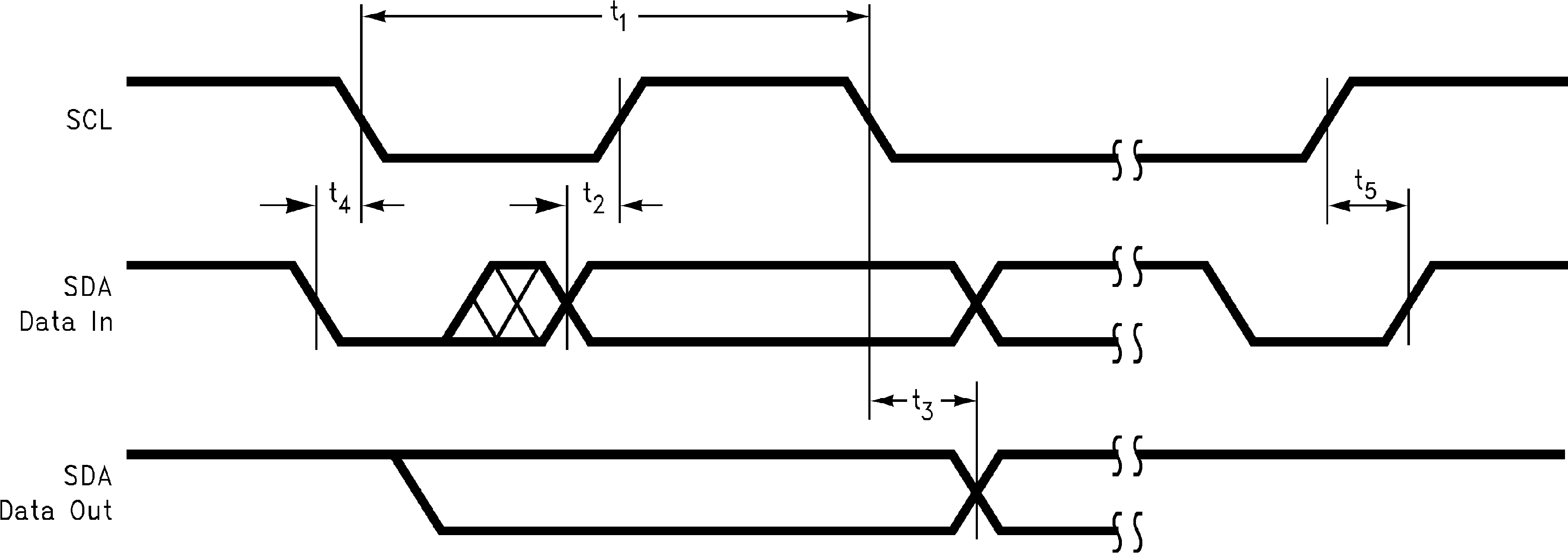 Figure 1. Serial Bus Timing Diagram
7.7 Typical Characteristics
The following typical performance plots apply for the internal VREF = 2.56 V, V+ = 3.3 V, Pseudo-Differential connection, unless otherwise specified. All limits TA = TJ = 25°C unless otherwise specified.A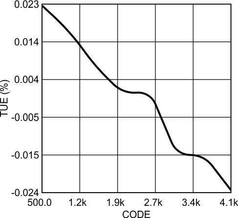 Figure 2. TUE vs. Code
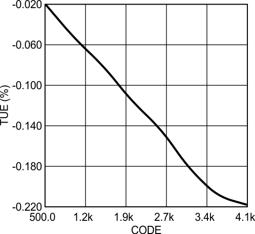 Figure 4. TUE vs. Code (External VREF = 2.56 V)
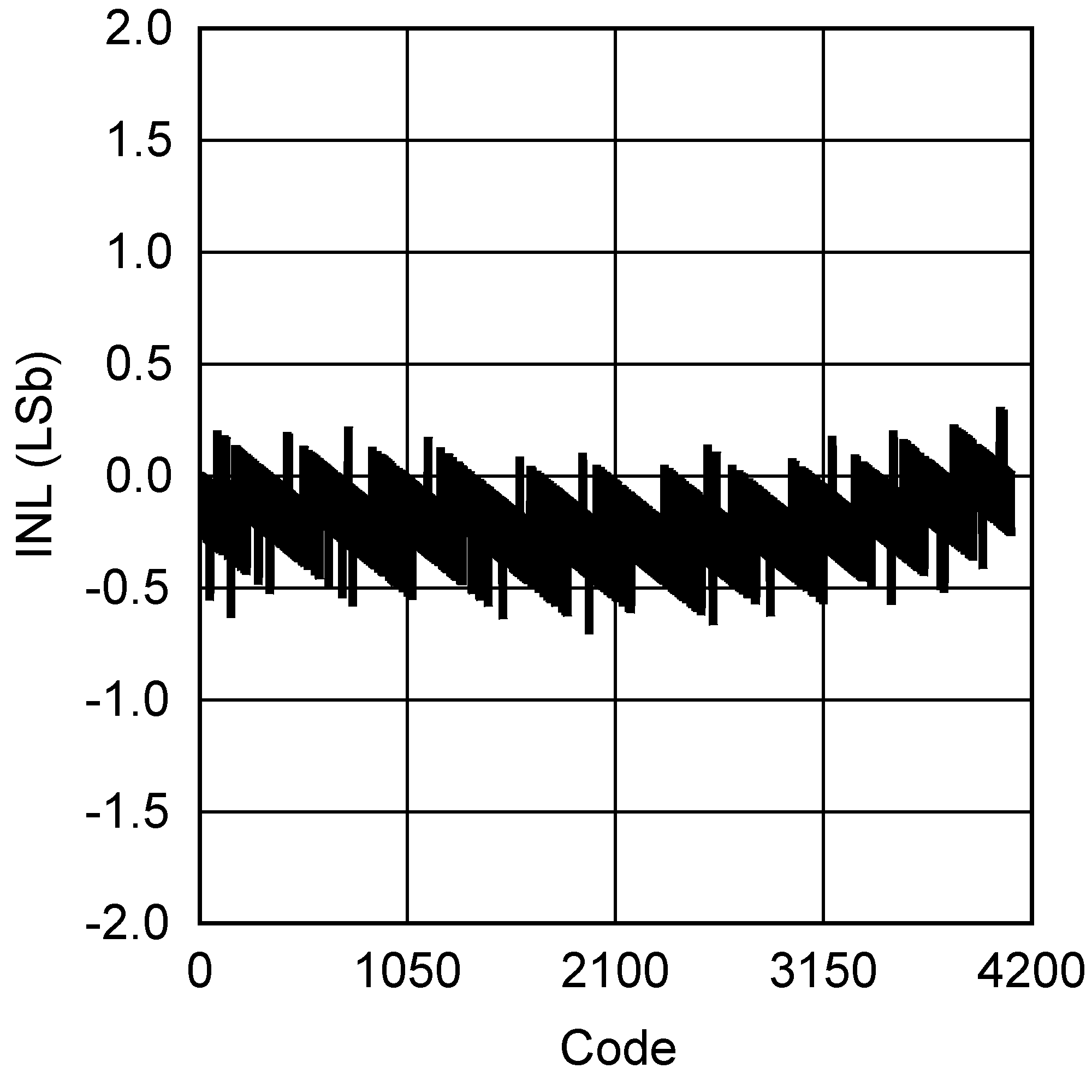 Figure 6. INL vs. Code (External VREF = 1.25 V for 1 Unit)
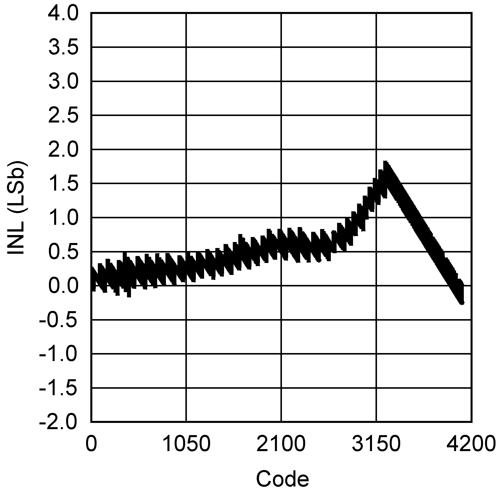 Figure 8. INL vs. Code (External VREF = 2.56 V for 1 Unit)
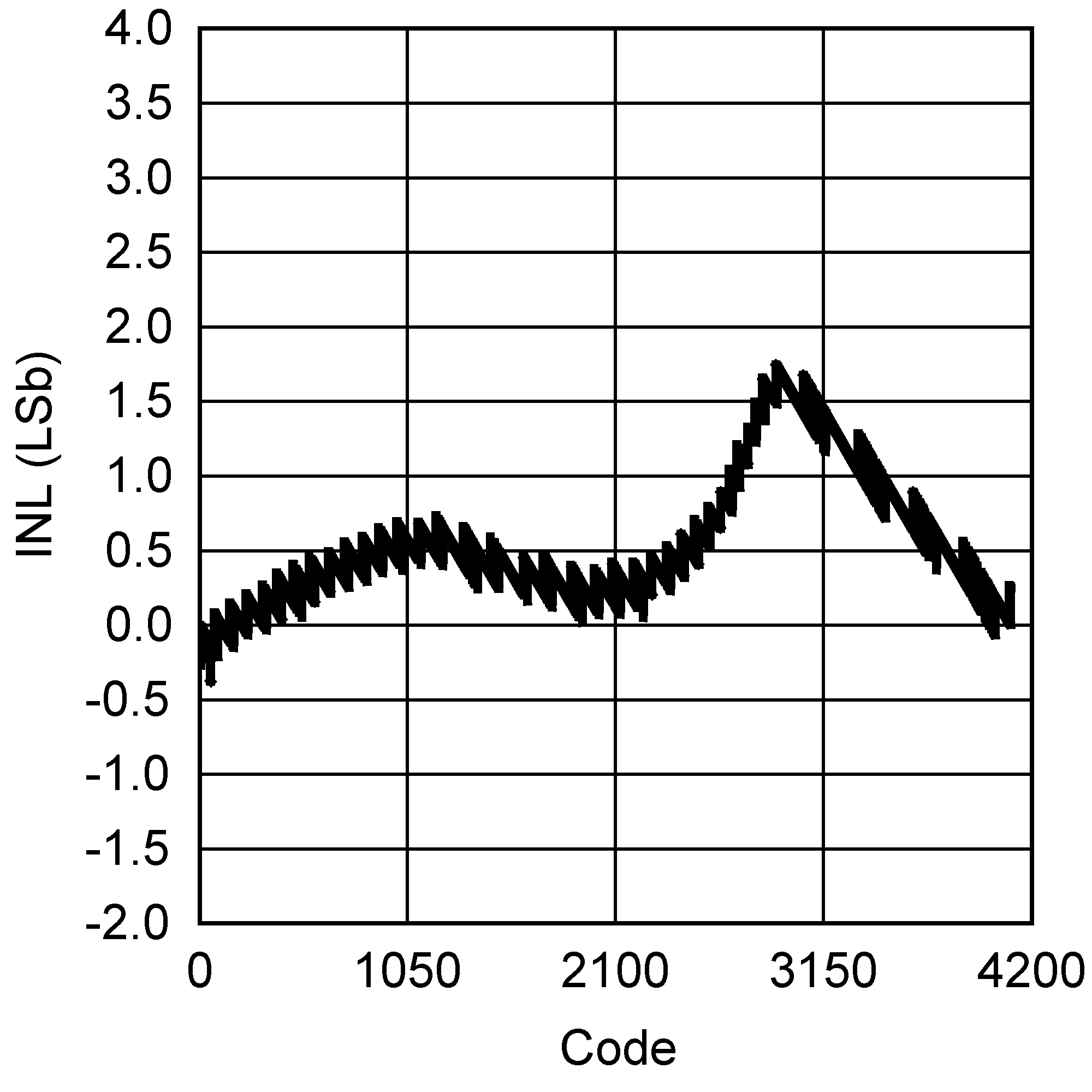 Figure 10. INL vs. Code (External VREF = 5 V, V+ = 5 V for 1 Unit)
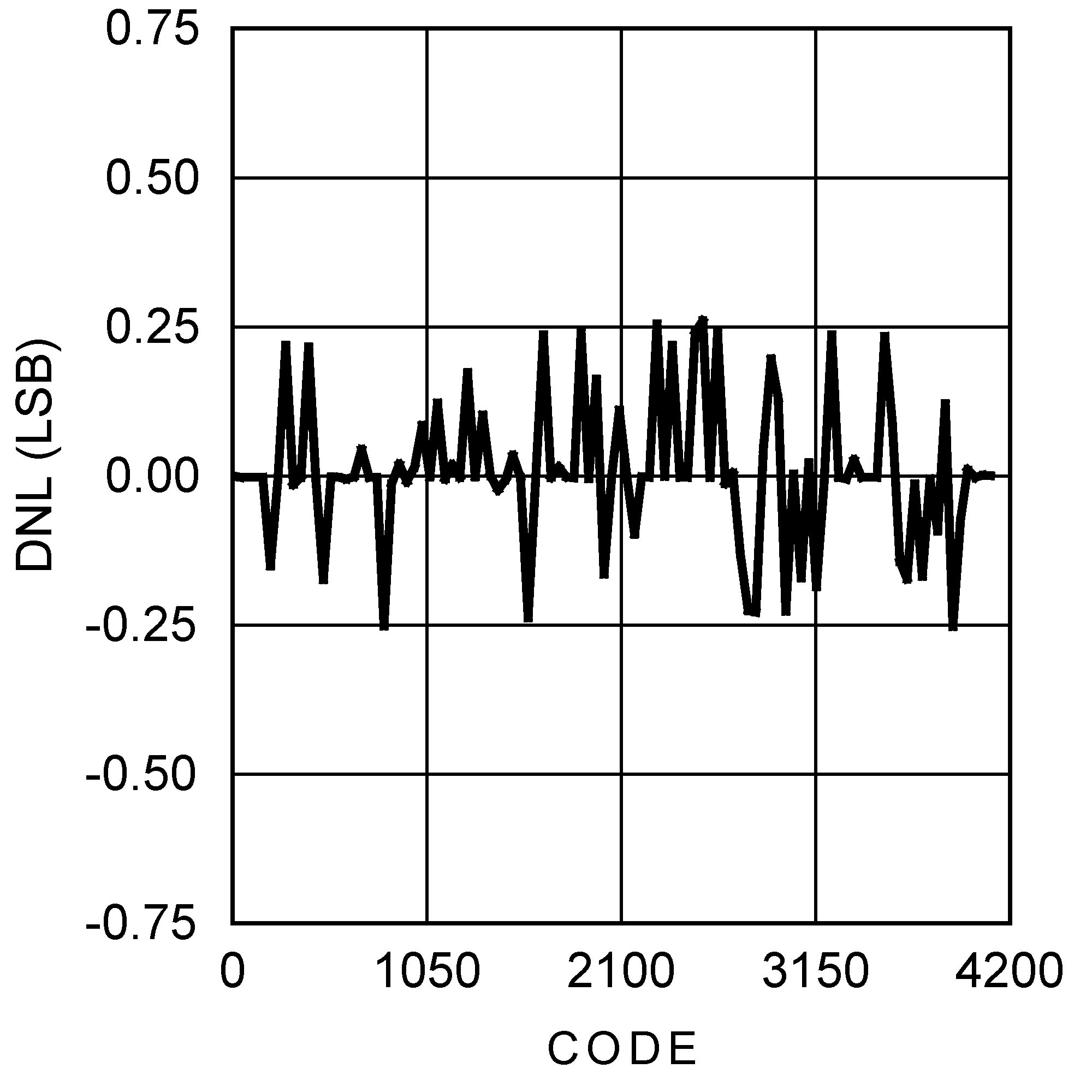 Figure 12. DNL vs. Code (External VREF = 2.56 V for 1 Unit)
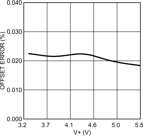 Figure 14. Offset Error vs. V+
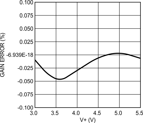 Figure 16. Gain Error vs. V+
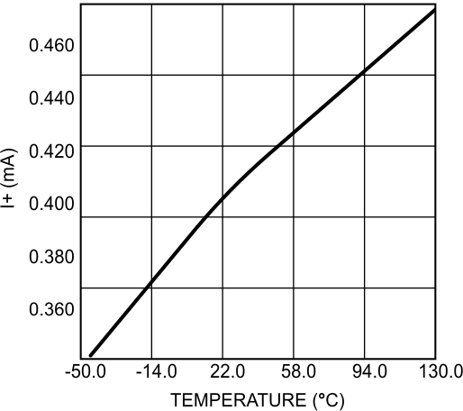 Figure 18. I+ vs. Temperature
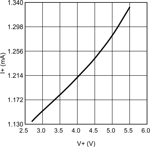 Figure 20. I+ vs. V+ for Voltage Conversion
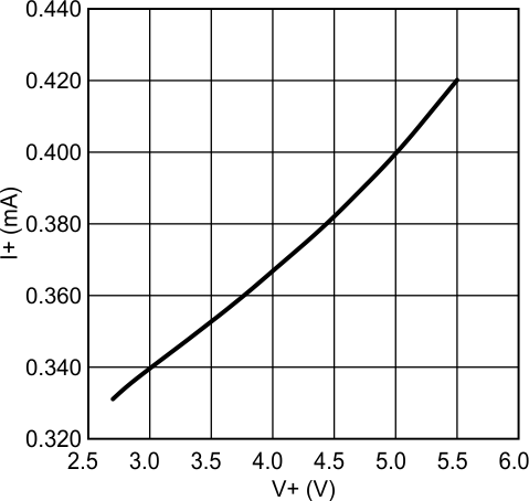 Figure 22. I+ vs. V+ in Shutdown Mode
 Figure 3. TUE vs. Code (External VREF = 1.25 V)
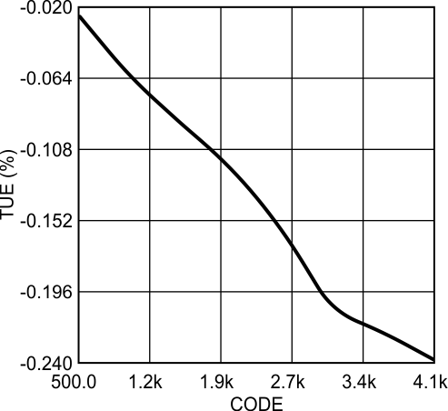 Figure 5. TUE vs. Code (External VREF = 5 V, V+ = 5 V)
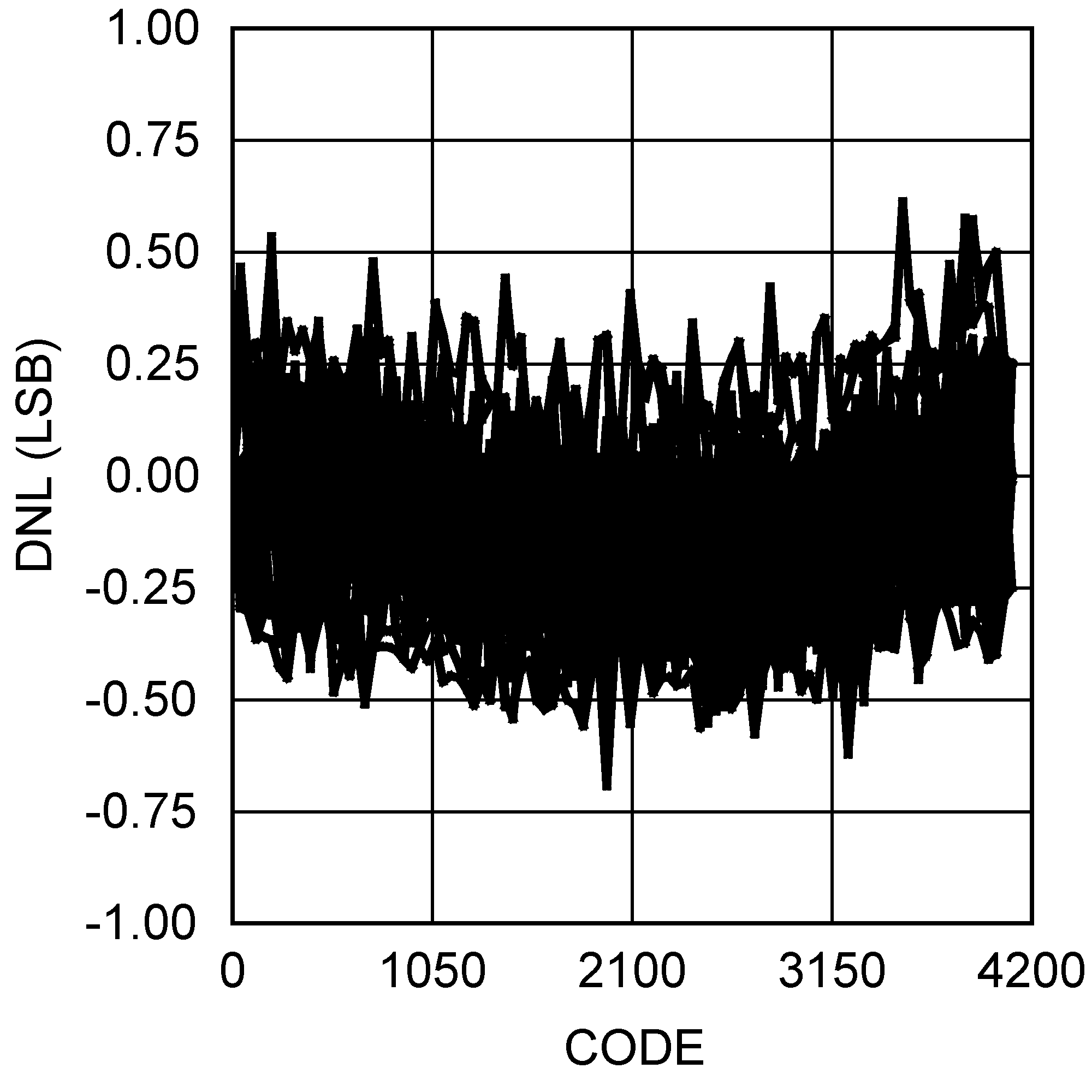 Figure 7. INL vs. Code (External VREF = 1.25 V for 28 Units)
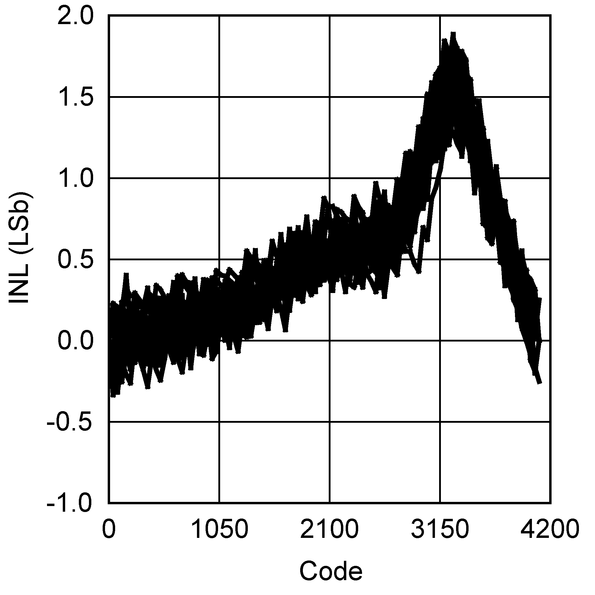 Figure 9. INL vs. Code (External VREF = 2.56 V for 28 Units)
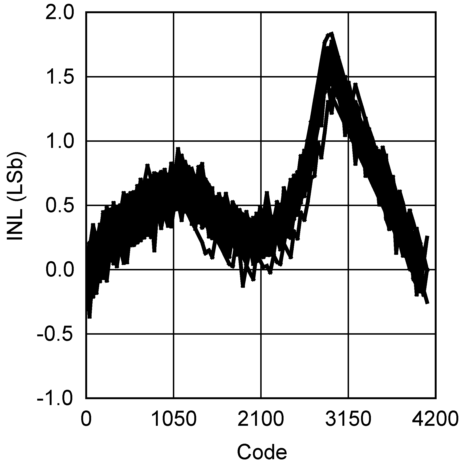 Figure 11. INL vs. Code (External VREF = 5 V, V+ = 5 V for 28 Units)
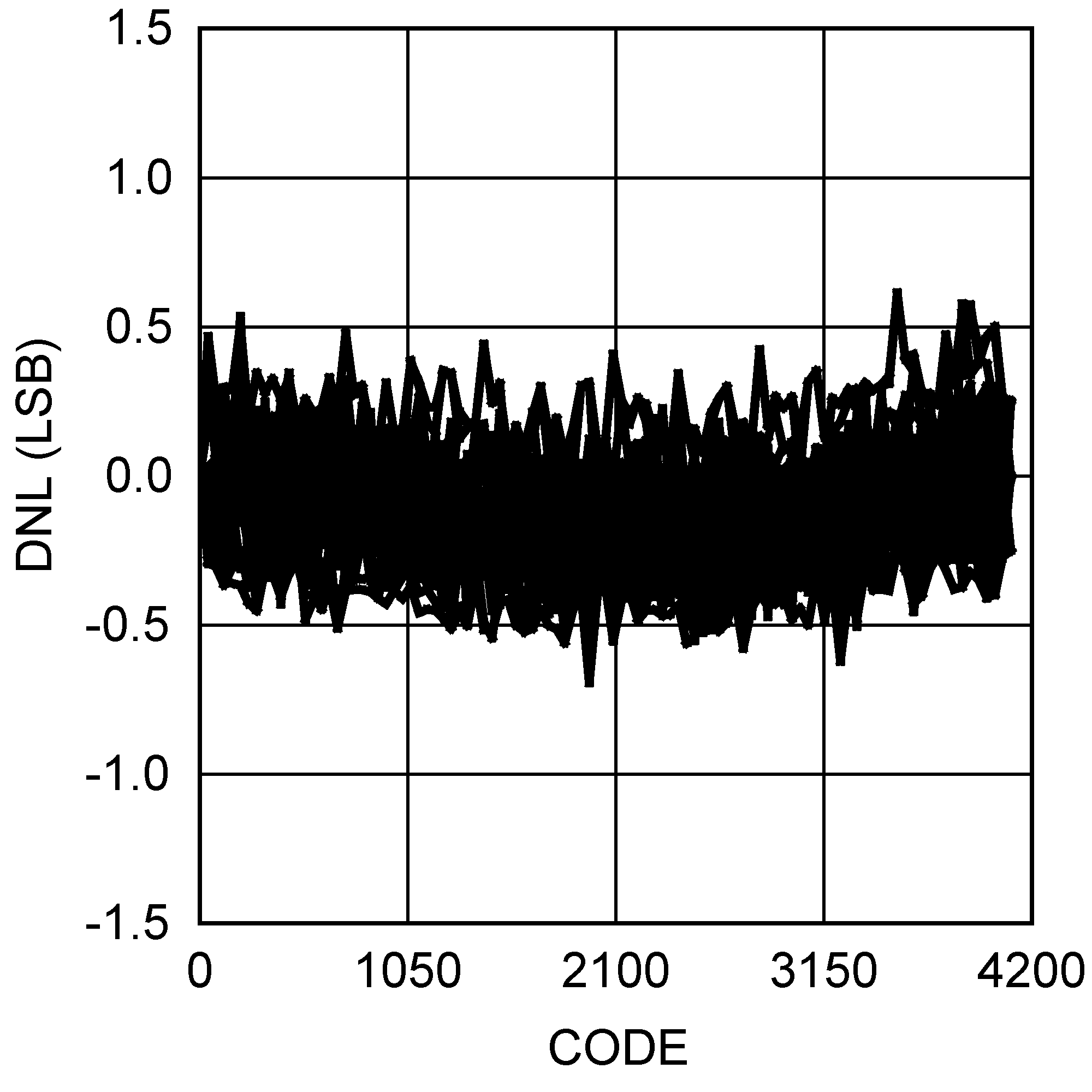 Figure 13. DNL vs. Code (External VREF = 2.56 V for 28 Units)
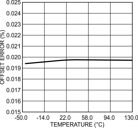 Figure 15. Offset Error vs. Temperature
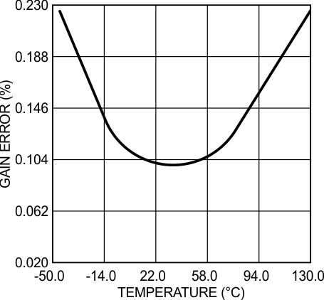 Figure 17. Gain Error vs. Temperature
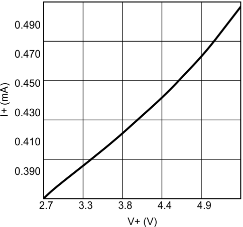 Figure 19. I+ vs. V+ Typical
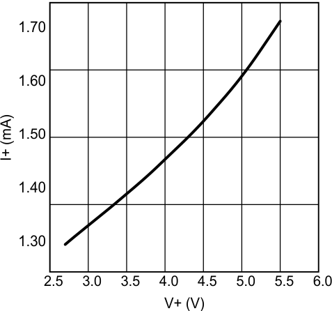 Figure 21. I+ vs. V+ for Temperature Conversion
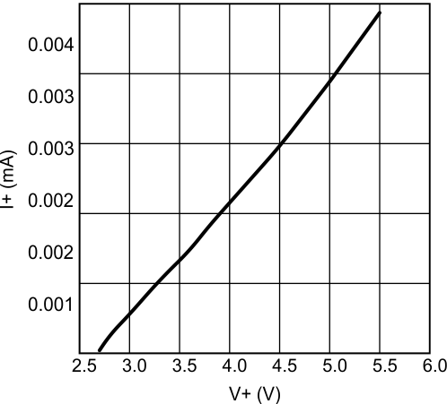 Figure 23. I+ vs. V+ in Deep Shutdown Mode
A. Timing specifications are tested at the Serial Bus Input logic levels: V IN(0) = 0.3 × V + for a falling edge and V IN(1) = 0.7 × V + for a rising edge if the SCL and SDA edge rates are similar