SNAS411P August 2008 – April 2017 ADC128S102QML-SP
PRODUCTION DATA.
- 1 Features
- 2 Applications
- 3 Description
- 4 Revision History
- 5 Pin Configuration and Functions
-
6 Specifications
- 6.1 Absolute Maximum Ratings
- 6.2 ESD Ratings
- 6.3 Recommended Operating Conditions
- 6.4 Thermal Information
- 6.5 Electrical Characteristics: ADC128S102QML-SP Converter
- 6.6 Electrical Characteristics: Radiation
- 6.7 Electrical Characteristics: Burn in Delta Parameters - TA at 25°C
- 6.8 Timing Requirements
- 6.9 Typical Characteristics
- 7 Detailed Description
- 8 Application and Implementation
- 9 Power Supply Recommendations
- 10Layout
- 11Device and Documentation Support
- 12Mechanical, Packaging, and Orderable Information
封装选项
请参考 PDF 数据表获取器件具体的封装图。
机械数据 (封装 | 引脚)
- NAC|16
- Y|0
- NAD|16
散热焊盘机械数据 (封装 | 引脚)
订购信息
7 Detailed Description
7.1 Overview
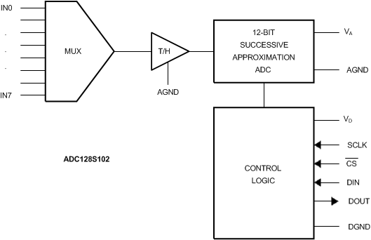
The ADC128S102 is a successive-approximation analog-to-digital converter designed around a charge redistribution digital-to-analog converter.
7.2 Functional Block Diagram
7.3 Feature Description
7.3.1 ADC128S102 Transfer Function
The output format of the ADC128S102 is straight binary. Code transitions occur midway between successive integer LSB values. The LSB width for the ADC128S102 is VA / 4096. The ideal transfer characteristic is shown in Figure 34. The transition from an output code of 0000 0000 0000 to a code of 0000 0000 0001 is at 1/2 LSB, or a voltage of VA / 8192. Other code transitions occur at steps of one LSB.
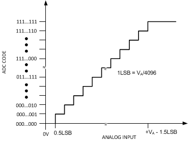 Figure 34. Ideal Transfer Characteristic
7.3.2 Analog Inputs
An equivalent circuit for one of the input channels of the ADC128S102 is shown in Figure 35. Diodes D1 and D2 provide ESD protection for the analog inputs. The operating range for the analog inputs is 0 V to VA. Going beyond this range will cause the ESD diodes to conduct and result in erratic operation.
The capacitor C1 in Figure 35 has a typical value of 3 pF and is mainly the package pin capacitance. Resistor R1 is the ON-resistance of the multiplexer and track or hold switch and is typically 500 Ω. Capacitor C2 is the ADC128S102 sampling capacitor, and is typically 30 pF. The ADC128S102 will deliver best performance when driven by a low-impedance source (less than 100 Ω). This is especially important when using the ADC128S102 to sample dynamic signals. Also important when sampling dynamic signals is a band-pass or low-pass filter which reduces harmonics and noise in the input. These filters are often referred to as anti-aliasing filters.
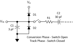 Figure 35. Equivalent Input Circuit
7.3.3 Digital Inputs and Outputs
The digital inputs of the ADC128S102 (SCLK, CS, and DIN) have an operating range of 0 V to VA. The inputs are not prone to latch-up and may be asserted before the digital supply (VD) without any risk. The digital output (DOUT) operating range is controlled by VD. The output high voltage is VD – 0.5 V (minimum) while the output low voltage is 0.4 V (maximum).
7.3.4 Radiation Environments
Careful consideration should be given to environmental conditions when using a product in a radiation environment.
7.3.4.1 Total Ionizing Dose
Radiation hardness assured (RHA) products are those part numbers with a total ionizing dose (TID) level listed in the Device Information table in the Description section. Testing and qualification of these products is done on a wafer level according to MIL-STD-883G, Test Method 1019.7. Testing is done according to Condition A and the Extended room temperature anneal test described in section 3.11 for application environment dose rates less than 0.027 rad(Si)/s. Wafer level TID data is available with lot shipments.
7.3.4.2 Single Event Latch-Up and Functional Interrupt
One-time single event latch-up (SEL) and single event functional interrupt (SEFI) testing was preformed according to EIA/JEDEC Standard, EIA/JEDEC57. The linear energy transfer threshold (LETth) shown in Features is the maximum LET tested. A test report is available upon request.
7.3.4.3 Single Event Upset
A report on single event upset (SEU) is available upon request.
7.4 Device Functional Modes
7.4.1 ADC128S102 Operation
Simplified schematics of the ADC128S102 in both track and hold operation are shown in Figure 36 and Figure 37 respectively. In Figure 36, the ADC128S102 is in track mode: switch SW1 connects the sampling capacitor to one of eight analog input channels through the multiplexer, and SW2 balances the comparator inputs. The ADC128S102 is in this state for the first three SCLK cycles after CS is brought low.
Figure 37 shows the ADC128S102 in hold mode: switch SW1 connects the sampling capacitor to ground, maintaining the sampled voltage, and switch SW2 unbalances the comparator. The control logic then instructs the charge-redistribution DAC to add or subtract fixed amounts of charge to or from the sampling capacitor until the comparator is balanced. When the comparator is balanced, the digital word supplied to the DAC is the digital representation of the analog input voltage. The ADC128S102 is in this state for the last thirteen SCLK cycles after CS is brought low.
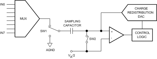 Figure 36. ADC128S102 in Track Mode
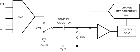 Figure 37. ADC128S102 in Hold Mode
7.5 Programming
7.5.1 Serial Interface
An operational timing diagram and a serial interface timing diagram for the ADC128S102 are shown in Figure 1 to Figure 3. CS, chip select, initiates conversions and frames the serial data transfers. SCLK (serial clock) controls both the conversion process and the timing of serial data. DOUT is the serial data output pin, where a conversion result is sent as a serial data stream, MSB first. Data to be written to the ADC128S102's Control Register is placed on DIN, the serial data input pin. New data is written to DIN with each conversion.
A serial frame is initiated on the falling edge of CS and ends on the rising edge of CS. Each frame must contain an integer multiple of 16 rising SCLK edges. The ADC's DOUT pin is in a high impedance state when CS is high and is active when CS is low. Note that CS is asynchronous. Thus, CS acts as an output enable. Similarly, SCLK is internally gated off when CS is brought high.
During the first 3 cycles of SCLK, the ADC is in the track mode, acquiring the input voltage. For the next 13 SCLK cycles the conversion is accomplished and the data is clocked out. SCLK falling edges 1 through 4 clock out leading zeros while falling edges 5 through 16 clock out the conversion result, MSB first. If there is more than one conversion in a frame (continuous conversion mode), the ADC will re-enter the track mode on the falling edge of SCLK after the N*16th rising edge of SCLK and re-enter the hold/convert mode on the N×16+4th falling edge of SCLK. "N" is an integer value.
The ADC128S102 enters track mode under three different conditions. In Figure 1, CS goes low with SCLK high and the ADC enters track mode on the first falling edge of SCLK. In the second condition, CS goes low with SCLK low. Under this condition, the ADC automatically enters track mode and the falling edge of CS is seen as the first falling edge of SCLK. In the third condition, CS and SCLK go low simultaneously and the ADC enters track mode. While there is no timing restriction with respect to the falling edges of CS and SCLK, see Figure 3 for setup and hold time requirements for the falling edge of CS with respect to the rising edge of SCLK.
During each conversion, data is clocked into a control register through the DIN pin on the first 8 rising edges of SCLK after the fall of CS. The control register is loaded with data indicating the input channel to be converted on the subsequent conversion (see Table 2, Table 3, and Table 4).
Although the ADC128S102 is able to acquire the input signal to full resolution in the first conversion immediately following power-up, the first conversion result after power-up will be that of a randomly selected channel. Therefore, the user needs to incorporate a dummy conversion to set the required channel that will be used on the subsequent conversion.
Table 2. Control Register Bits
| BIT 7 (MSB) | BIT 6 | BIT 5 | BIT 4 | BIT 3 | BIT 2 | BIT 1 | BIT 0 |
| DONTC | DONTC | ADD2 | ADD1 | ADD0 | DONTC | DONTC | DONTC |
Table 3. Control Register Bit Descriptions
| BIT | SYMBOL | DESCRIPTION |
|---|---|---|
| 7, 6, 2, 1, 0 | DONTC | Don't care. The values of these bits do not affect the device. |
| 5 | ADD2 | These three bits determine which input channel will be sampled and converted at the next conversion cycle. The mapping between codes and channels is shown in Table 4. |
| 4 | ADD1 | |
| 3 | ADD0 |
Table 4. Input Channel Selection
| ADD2 | ADD1 | ADD0 | INPUT CHANNEL |
|---|---|---|---|
| 0 | 0 | 0 | IN0 |
| 0 | 0 | 1 | IN1 |
| 0 | 1 | 0 | IN2 |
| 0 | 1 | 1 | IN3 |
| 1 | 0 | 0 | IN4 |
| 1 | 0 | 1 | IN5 |
| 1 | 1 | 0 | IN6 |
| 1 | 1 | 1 | IN7 |