SNAS518J July 2011 – July 2015 ADC12D1800RF
PRODUCTION DATA.
- 1 Device Overview
- 2 Revision History
- 3 Pin Configuration and Functions
-
4 Specifications
- 4.1 Absolute Maximum Ratings
- 4.2 ESD Ratings
- 4.3 Recommended Operating Conditions
- 4.4 Thermal Information
- 4.5 Converter Electrical Characteristics: Static Converter Characteristics
- 4.6 Converter Electrical Characteristics: Dynamic Converter Characteristics
- 4.7 Converter Electrical Characteristics: Analog Input / Output and Reference Characteristics
- 4.8 Converter Electrical Characteristics: I-Channel to Q-Channel Characteristics
- 4.9 Converter Electrical Characteristics: Sampling Clock Characteristics
- 4.10 Converter Electrical Characteristics: AutoSync Feature Characteristics
- 4.11 Converter Electrical Characteristics: Digital Control and Output Pin Characteristics
- 4.12 Converter Electrical Characteristics: Power Supply Characteristics
- 4.13 Converter Electrical Characteristics: AC Electrical Characteristics
- 4.14 Converter Electrical Characteristics: Serial Port Interface
- 4.15 Converter Electrical Characteristics Calibration
- 4.16 Typical Characteristics
-
5 Detailed Description
- 5.1 Overview
- 5.2 Functional Block Diagram
- 5.3 Feature Description
- 5.4 Device Functional Modes
- 5.5
Programming
- 5.5.1
Control Modes
- 5.5.1.1
Non-Extended Control Mode
- 5.5.1.1.1 Dual Edge Sampling Pin (DES)
- 5.5.1.1.2 Non-Demultiplexed Mode Pin (NDM)
- 5.5.1.1.3 Dual Data Rate Phase Pin (DDRPh)
- 5.5.1.1.4 Calibration Pin (CAL)
- 5.5.1.1.5 Calibration Delay Pin (CalDly)
- 5.5.1.1.6 Power Down I-channel Pin (PDI)
- 5.5.1.1.7 Power Down Q-channel Pin (PDQ)
- 5.5.1.1.8 Test Pattern Mode Pin (TPM)
- 5.5.1.1.9 Full-Scale Input Range Pin (FSR)
- 5.5.1.1.10 AC / DC-Coupled Mode Pin (VCMO)
- 5.5.1.1.11 LVDS Output Common-mode Pin (VBG)
- 5.5.1.2 Extended Control Mode
- 5.5.1.1
Non-Extended Control Mode
- 5.5.1
Control Modes
- 5.6 Register Maps
- 6 Application and Implementation
- 7 Power Supply Recommendations
- 8 Layout
- 9 Device and Documentation Support
- 10Mechanical, Packaging, and Orderable Information
8 Layout
8.1 Layout Guidelines
8.1.1 Power Planes
All supply buses for the ADC should be sourced from a common linear voltage regulator. This ensures that all power buses to the ADC are turned on and off simultaneously. This single source will be split into individual sections of the power plane, with individual decoupling and connection to the different power supply buses of the ADC. Due to the low voltage but relatively high supply current requirement, the optimal solution may be to use a switching regulator to provide an intermediate low voltage, which is then regulated down to the final ADC supply voltage by a linear regulator. Please refer to the documentation provided for the ADC12D1800RFRB for additional details on specific regulators that are recommended for this configuration.
Power for the ADC should be provided through a broad plane which is located on one layer adjacent to the ground plane(s). Placing the power and ground planes on adjacent layers will provide low impedance decoupling of the ADC supplies, especially at higher frequencies. The output of a linear regulator should feed into the power plane through a low impedance multi-via connection. The power plane should be split into individual power peninsulas near the ADC. Each peninsula should feed a particular power bus on the ADC, with decoupling for that power bus connecting the peninsula to the ground plane near each power / ground pin pair. Using this technique can be difficult on many printed circuit CAD tools. To work around this, zero ohm resistors can be used to connect the power source net to the individual nets for the different ADC power buses. As a final step, the zero ohm resistors can be removed and the plane and peninsulas can be connected manually after all other error checking is completed.
8.1.2 Bypass Capacitors
The general recommendation is to have one 100nF capacitor for each power / ground pin pair. The capacitors should be surface mount multi-layer ceramic chip capacitors similar to Panasonic part number ECJ-0EB1A104K.
8.1.3 Ground Planes
Grounding should be done using continuous full ground planes to minimize the impedance for all ground return paths, and provide the shortest possible image/return path for all signal traces.
8.1.4 Power System Example
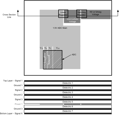
The ADC12D1800RFRB uses continuous ground planes (except where clear areas are needed to provide appropriate impedance management for specific signals), see Figure 8-1. Power is provided on one plane, with the 1.9V ADC supply being split into multiple zones or peninsulas for the specific power buses of the ADC. Decoupling capacitors are connected between these power bus peninsulas and the adjacent ground planes using vias. The capacitors are located as close to the individual power / ground pin pairs of the ADC as possible. In most cases, this means the capacitors are located on the opposite side of the PCB to the ADC.
 Figure 8-1 Power and Grounding Example
8.2 Layout Example
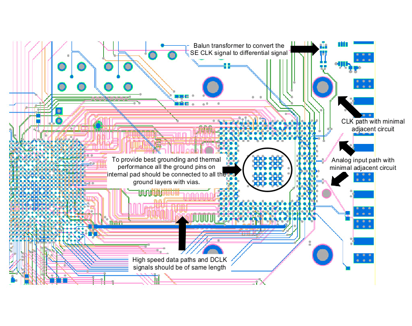
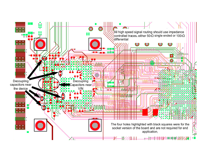
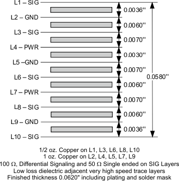
The following examples show layout-example plots. Figure 8-4 show a typical stack up for a 10 layer board.
 Figure 8-2 ADC12D1800RF Layout Example 1 - Top Side and Inner Layers
 Figure 8-3 ADC12D1800RF Layout Example 1 - Bottom Side and Inner Layers
 Figure 8-4 ADC12D1800RF Typical Stackup - 10 Layer Board
8.3 Thermal Management
The Heat Slug Ball Grid Array (HSBGA) package is a modified version of the industry standard plastic BGA (Ball Grid Array) package. Inside the package, a copper heat spreader cap is attached to the substrate top with exposed metal in the center top area of the package. This results in a 20% improvement (typical) in thermal performance over the standard plastic BGA package.
 Figure 8-5 HSBGA Conceptual Drawing
The center balls are connected to the bottom of the die by vias in the package substrate, Figure 8-5. This gives a low thermal resistance between the die and these balls. Connecting these balls to the PCB ground planes with a low thermal resistance path is the best way dissipate the heat from the ADC. These pins should also be connected to the ground plane via a low impedance path for electrical purposes. The direct connection to the ground planes is an easy method to spread heat away from the ADC. Along with the ground plane, the parallel power planes will provide additional thermal dissipation.
The center ground balls should be soldered down to the recommended ball pads (See SNOA021). These balls will have wide traces which in turn have vias which connect to the internal ground planes, and a bottom ground pad / pour if possible. This ensures a good ground is provided for these balls, and that the optimal heat transfer will occur between these balls and the PCB ground planes.
In spite of these package enhancements, analysis using the standard JEDEC JESD51-7 four-layer PCB thermal model shows that ambient temperatures must be limited to a max of 65°C to ensure a safe operating junction temperature for the ADC12D1800RF. However, most applications using the ADC12D1800RF will have a printed circuit board which is more complex than that used in JESD51-7. Typical circuit boards will have more layers than the JESD51-7 (eight or more), several of which will be used for ground and power planes. In those applications, the thermal resistance parameters of the ADC12D1800RF and the circuit board can be used to determine the actual safe ambient operating temperature up to a maximum of 85°C.
Three key parameters are provided to allow for modeling and calculations. Because there are two main thermal paths between the ADC die and external environment, the thermal resistance for each of these paths is provided. θJC1 represents the thermal resistance between the die and the exposed metal area on the top of the HSBGA package. θJC2 represents the thermal resistance between the die and the center group of balls on the bottom of the HSBGA package. The final parameter is the allowed maximum junction temperature, which is TJ.
In other applications, a heat sink or other thermally conductive path can be added to the top of the HSBGA package to remove heat. In those cases, θJC1 can be used along with the thermal parameters for the heat sink or other thermal coupling added. Representative heat sinks which might be used with the ADC12D1800RF include the Cool Innovations p/n 3-1212XXG and similar products from other vendors. In many applications, the printed circuit board will provide the primary thermal path conducting heat away from the ADC package. In those cases, θJC2 can be used in conjunction with printed circuit board thermal modeling software to determine the allowed operating conditions that will maintain the die temperature below the maximum allowable limit. Additional dissipation can be achieved by coupling a heat sink to the copper pour area on the bottom side of the printed circuit board.
Typically, dissipation will occur through one predominant thermal path. In these cases, the following calculations can be used to determine the maximum safe ambient operating temperature:
TJ = TA + PD × (θJC+θCA)
TJ = TA + PC(MAX) × (θJC+θCA)
For θJC, the value for the primary thermal path in the given application environment should be used (θJC1 or θJC2). θCA is the thermal resistance from the case to ambient, which would typically be that of the heat sink used. Using this relationship and the desired ambient temperature, the required heat sink thermal resistance can be found. Alternately, the heat sink thermal resistance can be used to find the maximum ambient temperature. For more complex systems, thermal modeling software can be used to evaluate the printed circuit board system and determine the expected junction temperature given the total system dissipation and ambient temperature.