ZHCSOI5A October 2021 – November 2024 ADC12DJ1600 , ADC12QJ1600 , ADC12SJ1600
PRODUCTION DATA
- 1
- 1 特性
- 2 应用
- 3 说明
- 4 Device Comparison
- 5 Pin Configuration and Functions
-
6 Specifications
- 6.1 Absolute Maximum Ratings
- 6.2 ESD Ratings
- 6.3 Recommended Operating Conditions
- 6.4 Thermal Information
- 6.5 Electrical Characteristics: DC Specifications
- 6.6 Electrical Characteristics: Power Consumption
- 6.7 Electrical Characteristics: AC Specifications
- 6.8 Timing Requirements
- 6.9 Switching Characteristics
- 6.10 Typical Characteristics
-
7 Detailed Description
- 7.1 Overview
- 7.2 Functional Block Diagram
- 7.3
Feature Description
- 7.3.1 Analog Input
- 7.3.2 Temperature Monitoring Diode
- 7.3.3 Timestamp
- 7.3.4 Clocking
- 7.3.5
JESD204C Interface
- 7.3.5.1 Transport Layer
- 7.3.5.2 Scrambler
- 7.3.5.3 Link Layer
- 7.3.5.4 8B or 10B Link Layer
- 7.3.5.5 64B or 66B Link Layer
- 7.3.5.6 Physical Layer
- 7.3.5.7 JESD204C Enable
- 7.3.5.8 Multi-Device Synchronization and Deterministic Latency
- 7.3.5.9 Operation in Subclass 0 Systems
- 7.3.5.10 Alarm Monitoring
- 7.4
Device Functional Modes
- 7.4.1 Low Power Mode and High Performance Mode
- 7.4.2 JESD204C Modes
- 7.4.3 Power-Down Modes
- 7.4.4 Test Modes
- 7.4.5 Calibration Modes and Trimming
- 7.4.6 Offset Calibration
- 7.4.7 Trimming
- 7.5 Programming
- 8 Application and Implementation
- 9 Device and Documentation Support
- 10Revision History
- 11Mechanical, Packaging, and Orderable Information
7.3.5 JESD204C Interface
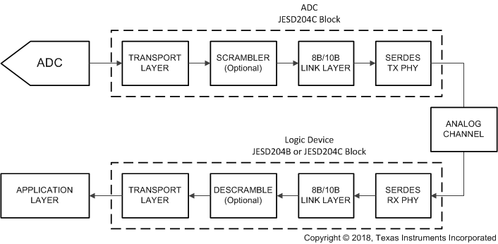
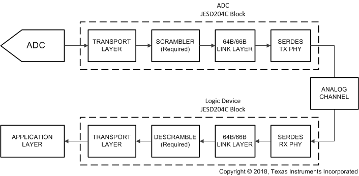
The device uses a JESD204C high-speed serial interface for data converters to transfer data from the ADC to the receiving logic device. The device serialized lanes are capable of operating with both 8B/10B encoding and 64B or 66B encoding. The JESD204C output formats using 8B or 10B encoding are backwards compatible with existing JESD204B receivers. A maximum of 8 lanes can be used to lower lane rates for interfacing with speed-limited logic devices. There are a few differences between 8B or 10B and 64B or 66B encoded JESD204C, which is highlighted throughout this section. Figure 7-7 shows a simplified block diagram of the 8B or 10B encoded JESD204C interface and Figure 7-8 shows a simplified block diagram of the 64B or 66B encoded JESD204C interface.
 Figure 7-7 Simplified 8B/10B Encoded JESD204C Interface Diagram
 Figure 7-8 Simplified 64B/66B Encoded JESD204C Interface Diagram
The various signals used in the JESD204C interface and the associated ADC12QJ1600 pin names are summarized briefly in Table 7-7 for reference. Most of the signals are common between 8B or 10B and 64B or 66B encoded JESD204C, except for SYNC which is not needed to achieve block synchronization for 64B or 66B encoding. The sync header encoded into the data stream is used for block synchronization instead of the SYNC signal.
| SIGNAL NAME | PIN NAMES | 8B/10B | 64B/66B | DESCRIPTION |
|---|---|---|---|---|
| Data | Quad/dual channel: D[7:0]+, D[7:0]– Single channel: D[3:0]+, D[3:0]– | Yes | Yes | High-speed serialized data after 8B/10B or 64B/66B encoding |
| SYNC | SYNCSE | Yes | No | Link initialization signal (handshake), toggles low to start code group synchronization (CGS) process. Not used for 64B/66B encoding modes, unless it is used for NCO synchronization purposes. |
| Device clock | CLK+, CLK– or SE_CLK | Yes | Yes | ADC sampling clock or PLL reference clock, also used for clocking digital logic and output serializers |
| SYSREF | SYSREF+, SYSREF– | Yes | Yes | System timing reference used to deterministically reset the internal local multiframe clock (LMFC) or local extended multiblock clock (LEMC) counters in each JESD204C device |
Not all optional features of JESD204C are supported by ADC12QJ1600. The list of features that are supported and the features that are not supported is provided in Table 7-8.
| LETTER IDENTIFIER | REFERENCE CLAUSE | FEATURE | SUPPORT IN ADC12QJ1600 |
|---|---|---|---|
| a | clause 8 | 8B/10B link layer | Supported |
| b | clause 7 | 64B/66B link layer | Supported |
| c | clause 7 | 64B/80B link layer | Not supported |
| d | clause 7 | The command channel when using the 64B/66B or 64B/80B link layer | Not supported |
| e | clause 7 | Forward error correction (FEC) when using the 64B/66B or 64B/80B link layer | Supported |
| f | clause 7 | CRC3 when using the 64B/66B or 64B/80B link layer | Not supported |
| g | clause 8 | A physical SYNC pin when using the 8B/10B link layer | Supported |
| h | clause 7, clause 8 | Subclass 0 | Not supported, but subclass 1 transmitter is compatible with subclass 0 receiver |
| i | clause 7, clause 8 | Subclass 1 | Supported |
| j | clause 8 | Subclass 2 | Not supported |
| k | clause 7, clause 8 | Lane alignment within a single link | Supported |
| l | clause 7, clause 8 | Subclass 1 with support for a lane alignment on a multipoint link by means of the MULTIREF signal | Not supported |
| m | clause 8 | SYNC interface timing is compatible with JESD204A | Supported |
| n | clause 8 | SYNC interface timing is compatible with JESD204B | Supported |