ZHCSP07A
October 2021 – October 2024
ADC12DJ800
,
ADC12QJ800
,
ADC12SJ800
PRODUCTION DATA
1
1
特性
2
应用
3
说明
4
Pin Configuration and Functions
5
Specifications
5.1
Absolute Maximum Ratings
5.2
ESD Ratings
5.3
Recommended Operating Conditions
5.4
Thermal Information
5.5
Electrical Characteristics: DC Specifications
5.6
Electrical Characteristics: Power Consumption
5.7
Electrical Characteristics: AC Specifications
5.8
Timing Requirements
5.9
Switching Characteristics
5.10
Typical Characteristics
6
Detailed Description
6.1
Overview
6.2
Functional Block Diagram
6.3
Feature Description
6.3.1
Device Comparison
6.3.2
Analog Input
6.3.2.1
Analog Input Protection
6.3.2.2
Full-Scale Voltage (VFS) Adjustment
6.3.2.3
Analog Input Offset Adjust
6.3.2.4
ADC Core
6.3.2.4.1
ADC Theory of Operation
6.3.2.4.2
ADC Core Calibration
6.3.2.4.3
Analog Reference Voltage
6.3.2.4.4
ADC Over-range Detection
6.3.2.4.5
Code Error Rate (CER)
6.3.3
Temperature Monitoring Diode
6.3.4
Timestamp
6.3.5
Clocking
6.3.5.1
Converter PLL (C-PLL) for Sampling Clock Generation
6.3.5.2
LVDS Clock Outputs (PLLREFO±, TRIGOUT±)
6.3.5.3
Optional CMOS Clock Outputs (ORC, ORD)
6.3.5.4
SYSREF for JESD204C Subclass-1 Deterministic Latency
6.3.5.4.1
SYSREF Capture for Multi-Device Synchronization and Deterministic Latency
6.3.5.4.2
SYSREF Position Detector and Sampling Position Selection (SYSREF Windowing)
6.3.6
JESD204C Interface
6.3.6.1
Transport Layer
6.3.6.2
Scrambler
6.3.6.3
Link Layer
6.3.6.4
8B/10B Link Layer
6.3.6.4.1
Data Encoding (8B/10B)
6.3.6.4.2
Multiframes and the Local Multiframe Clock (LMFC)
6.3.6.4.3
Code Group Synchronization (CGS)
6.3.6.4.4
Initial Lane Alignment Sequence (ILAS)
6.3.6.4.5
Frame and Multiframe Monitoring
6.3.6.5
64B/66B Link Layer
6.3.6.5.1
64B/66B Encoding
6.3.6.5.2
Multiblocks, Extended Multiblocks and the Local Extended Multiblock Clock (LEMC)
6.3.6.5.2.1
Block, Multiblock and Extended Multiblock Alignment using Sync Header
6.3.6.5.2.1.1
Cyclic Redundancy Check (CRC) Mode
6.3.6.5.2.1.2
Forward Error Correction (FEC) Mode
6.3.6.5.3
Initial Lane Alignment
6.3.6.5.4
Block, Multiblock and Extended Multiblock Alignment Monitoring
6.3.6.6
Physical Layer
6.3.6.6.1
SerDes Pre-Emphasis
6.3.6.7
JESD204C Enable
6.3.6.8
Multi-Device Synchronization and Deterministic Latency
6.3.6.9
Operation in Subclass 0 Systems
6.3.6.10
Alarm Monitoring
6.3.6.10.1
Clock Upset Detection
6.3.6.10.2
FIFO Upset Detection
6.4
Device Functional Modes
6.4.1
Low Power Mode and High Performance Mode
6.4.2
JESD204C Modes
6.4.2.1
JESD204C Transport Layer Data Formats
6.4.2.2
64B/66B Sync Header Stream Configuration
6.4.2.3
Redundant Data Mode (Alternate Lanes)
6.4.3
Power-Down Modes
6.4.4
Test Modes
6.4.4.1
Serializer Test-Mode Details
6.4.4.2
PRBS Test Modes
6.4.4.3
Clock Pattern Mode
6.4.4.4
Ramp Test Mode
6.4.4.5
Short and Long Transport Test Mode
6.4.4.5.1
Short Transport Test Pattern
6.4.4.6
D21.5 Test Mode
6.4.4.7
K28.5 Test Mode
6.4.4.8
Repeated ILA Test Mode
6.4.4.9
Modified RPAT Test Mode
6.4.5
Calibration Modes and Trimming
6.4.5.1
Foreground Calibration Mode
6.4.5.2
Background Calibration Mode
6.4.5.3
Low-Power Background Calibration (LPBG) Mode
6.4.6
Offset Calibration
6.4.7
Trimming
6.5
Programming
6.5.1
Using the Serial Interface
6.5.2
SCS
6.5.3
SCLK
6.5.4
SDI
6.5.5
SDO
6.5.6
Streaming Mode
6.5.7
SPI_Register_Map Registers
7
Application and Implementation
7.1
Application Information
7.2
Typical Applications
7.2.1
Light Detection and Ranging (LiDAR) Digitizer
7.2.1.1
Design Requirements
7.2.1.2
Detailed Design Procedure
7.2.1.2.1
Analog Front-End Requirements
7.2.1.2.2
Calculating Clock and SerDes Frequencies
7.2.1.3
Application Curves
7.3
Initialization Set Up
7.4
Power Supply Recommendations
7.4.1
Power Sequencing
7.5
Layout
7.5.1
Layout Guidelines
7.5.2
Layout Example
8
Device and Documentation Support
8.1
Device Support
8.2
接收文档更新通知
8.3
支持资源
8.4
Trademarks
8.5
静电放电警告
8.6
术语表
9
Revision History
10
Mechanical, Packaging, and Orderable Information
封装选项
机械数据 (封装 | 引脚)
AAV|144
MPBGAM2C
散热焊盘机械数据 (封装 | 引脚)
订购信息
zhcsp07a_oa
zhcsp07a_pm
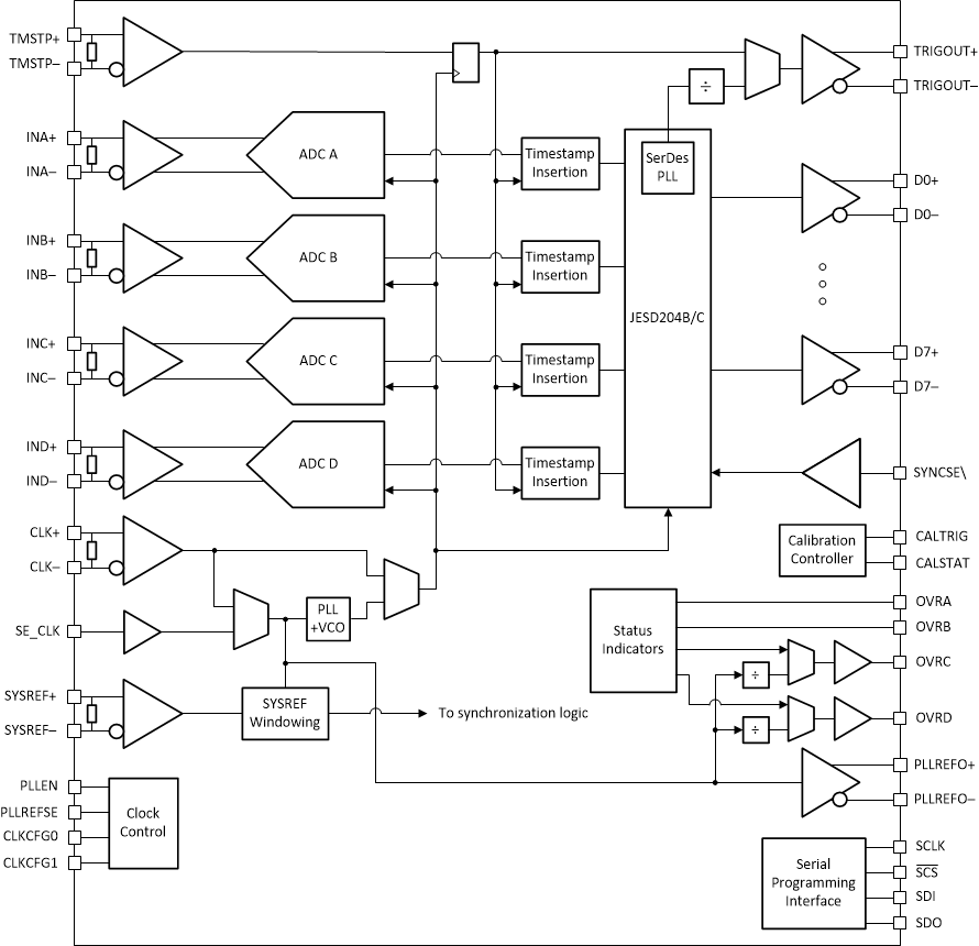
6.2
Functional Block Diagram
Figure 6-1
Quad Channel Functional Block Diagram
Figure 6-2
Dual Channel Functional Block Diagram
Figure 6-3
Single Channel Functional Block Diagram
千亿体育app官网登录(中国)官方网站IOS/安卓通用版/手机APP
|
米乐app下载官网(中国)|ios|Android/通用版APP最新版
|
米乐|米乐·M6(中国大陆)官方网站
|
千亿体育登陆地址
|
华体会体育(中国)HTH·官方网站
|
千赢qy国际_全站最新版千赢qy国际V6.2.14安卓/IOS下载
|
18新利网v1.2.5|中国官方网站
|
bob电竞真人(中国官网)安卓/ios苹果/电脑版【1.97.95版下载】
|
千亿体育app官方下载(中国)官方网站IOS/安卓/手机APP下载安装
|