ZHCSHX9L November 2008 – February 2019 ADC14155QML-SP
PRODUCTION DATA.
- 1 特性
- 2 应用
- 3 说明
- 4 修订历史记录
- 5 Pin Configuration and Functions
-
6 Specifications
- 6.1 Absolute Maximum Ratings
- 6.2 ESD Ratings
- 6.3 Recommended Operating Conditions
- 6.4 Thermal Information
- 6.5 ADC14155 Converter Electrical Characteristics DC Parameters
- 6.6 ADC14155 Converter Electrical Characteristics (Continued) DYNAMIC Parameters
- 6.7 ADC14155 Converter Electrical Characteristics (Continued) Logic and Power Supply Electrical Characteristics
- 6.8 ADC14155 Converter Electrical Characteristics (Continued) Timing and AC Characteristics
- 6.9 Timing Diagram
- 6.10 Transfer Characteristic
- 6.11 Typical Performance Characteristics, DNL, INL
- 6.12 Typical Performance Characteristics, Dynamic Performance
- 7 Detailed Description
- 8 Application and Implementation
- 9 Power Supply Recommendations
- 10Layout
- 11器件和文档支持
- 12机械、封装和可订购信息
6.6 ADC14155 Converter Electrical Characteristics (Continued) DYNAMIC Parameters(11)
Unless otherwise specified, the following specifications apply: AGND = DGND = DRGND = 0 V, VA = VD = 3.3 V, VDR = 1.8 V, Internal VREF = 1 V, fCLK = 155 MHz, VCM = VRM, CL = 5 pF/pin, Differential Analog Input, Single-Ended Clock Mode, Offset Binary Format. Typical values are for TA = 25°C. (1)(4)(5)(2)| PARAMETER | TEST CONDITIONS | NOTES | TYP(6) | MIN | MAX | UNITS | SUB-GROUPS | |
|---|---|---|---|---|---|---|---|---|
| DYNAMIC CONVERTER CHARACTERISTICS, AIN = -1 dBFS | ||||||||
| FPBW | Full power bandwidth | -1 dBFS Input, -3 dB Corner | 1.1 | GHz | ||||
| SNR | Signal-to-noise ratio | fIN = 10 MHz | 69 | dBFS | ||||
| fIN = 70 MHz | 70.1 | 66.7 | dBFS | |||||
| fIN = 169 MHz | 68.5 | dBFS | ||||||
| fIN = 238 MHz | 68.5 | dBFS | ||||||
| fIN = 398 MHz | 66.4 | dBFS | ||||||
| SFDR | Spurious free dynamic range | fIN = 10 MHz | 82 | dBFS | ||||
| fIN = 70 MHz | 82.3 | 68.2 | dBFS | |||||
| fIN = 169 MHz | 80.5 | dBFS | ||||||
| fIN = 238 MHz | 77.3 | dBFS | ||||||
| fIN = 398 MHz | 63.5 | dBFS | ||||||
| ENOB | Effective number of bits | fIN = 10 MHz | 11.3 | Bits | ||||
| fIN = 70 MHz | 11.3 | 10.7 | Bits | |||||
| fIN = 169 MHz | 11.0 | Bits | ||||||
| fIN = 238 MHz | 11.0 | Bits | ||||||
| fIN = 398 MHz | 10.0 | Bits | ||||||
| THD | Total harmonic disortion | fIN = 10 MHz | –81 | dBFS | ||||
| fIN = 70 MHz | –79.9 | –67 | dBFS | |||||
| fIN = 169 MHz | –82.4 | dBFS | ||||||
| fIN = 238 MHz | –76.6 | dBFS | ||||||
| fIN = 398 MHz | –63.2 | dBFS | ||||||
| HD2 | Second-order harmonic distortion | fIN = 10 MHz | –95.4 | dBFS | ||||
| fIN = 70 MHz | –88.5 | –70 | dBFS | |||||
| fIN = 169 MHz | –88.3 | dBFS | ||||||
| fIN = 238 MHz | –77.3 | dBFS | ||||||
| fIN = 398 MHz | –60.9 | dBFS | ||||||
| HD3 | Third-order harmonic distortion | fIN = 10 MHz | –81.6 | dBFS | ||||
| fIN = 70 MHz | –82.3 | –68 | dBFS | |||||
| fIN = 169 MHz | –86.4 | dBFS | ||||||
| fIN = 238 MHz | –89.0 | dBFS | ||||||
| fIN = 398 MHz | –80.5 | dBFS | ||||||
| SINAD | Signal-to-noise and distortion ratio | fIN = 10 MHz | 68.2 | dBFS | ||||
| fIN = 70 MHz | 69.9 | 66.2 | dBFS | |||||
| fIN = 169 MHz | 68.3 | dBFS | ||||||
| fIN = 238 MHz | 67.8 | dBFS | ||||||
| fIN = 398 MHz | 61.5 | dBFS | ||||||
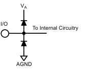
(1) The inputs are protected as shown below. Input voltage magnitudes above VA or below GND will not damage this device, provided current is limited per Note 5. However, errors in the A/D conversion can occur if the input goes above 2.6V or below GND as described in the Recommended Operating Conditions section.


(2) When the input voltage at any pin exceeds the power supplies (that is, VIN < AGND, or VIN > VA), the current at that pin should be limited to ±5 mA. The ±50 mA maximum package input current rating limits the number of pins that can safely exceed the power supplies with an input current of ±5 mA to 10.