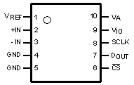
| 1 |
VREF |
Reference input |
Voltage reference input. A voltage reference between 1 V and VA must be applied to this input. VREF must be decoupled to GND with a minimum ceramic capacitor value of 0.1 µF. A bulk capacitor value of 1.0 µF to 10 µF in parallel with the 0.1-µF capacitor is recommended for enhanced performance. |
| 2 |
+IN |
Analog signal input, positive |
Noninverting input. +IN is the positive analog input for the signal applied to the ADC141S628-Q1. |
| 3 |
–IN |
Analog signal input, negative |
Inverting input. Must be GND ± 150 mV. |
| 4 |
GND |
Supply |
Ground. GND is the ground reference point for all signals applied to the ADC141S628-Q1. |
| 5 |
GND |
Supply |
Ground. GND is the ground reference point for all signals applied to the ADC141S628-Q1. |
| 6 |
CS |
Digital input |
Chip-select bar. CS must be active LOW during an SPI conversion, which begins on the falling edge of CS. The ADC141S628-Q1 is in acquisition mode when CS is HIGH. |
| 7 |
DOUT |
Digital output |
Serial data output. The conversion result is provided on DOUT. The serial data output word is comprised of two null bits followed by 14 data bits (MSB first). During a conversion, the data are output on the falling edges of SCLK and are valid on the subsequent rising edges. |
| 8 |
SCLK |
Digital input |
Serial clock. SCLK is used to control data transfer and serves as the conversion clock. |
| 9 |
VIO |
Supply |
Digital input/output power-supply input. A voltage source between 4.5 V and 5.5 V must be applied to this input. VIO must be decoupled to GND with a minimum ceramic capacitor value of 0.1 µF. |
| 10 |
VA |
Supply |
Analog power-supply input. A voltage source between 4.5 V and 5.5 V must be applied to this input. VA must be decoupled to GND with a minimum ceramic capacitor value of 0.1 µF. |
