ZHCSCD9C April 2014 – August 2014 ADC16DX370
PRODUCTION DATA.
- 1 特性
- 2 应用范围
- 3 说明
- 4 修订历史记录
- 5 Pin Configuration and Functions
-
6 Specifications
- 6.1 Absolute Maximum Ratings
- 6.2 Handling Ratings
- 6.3 Recommended Operating Conditions
- 6.4 Thermal Information
- 6.5 Converter Performance Characteristics
- 6.6 Power Supply Electrical Characteristics
- 6.7 Analog Interface Electrical Characteristics
- 6.8 CLKIN, SYSREF, SYNCb Interface Electrical Characteristics
- 6.9 Serial Data Output Interface Electrical Characteristics
- 6.10 Digital Input Electrical Interface Characteristics
- 6.11 Timing Requirements
- 6.12 Typical Characteristics
- 7 Parameter Measurement Information
-
8 Detailed Description
- 8.1 Overview
- 8.2 Functional Block Diagram
- 8.3
Feature Description
- 8.3.1 Amplitude and Phase Imbalance Correction of Differential Analog Input
- 8.3.2 DC Offset Correction
- 8.3.3 Over-Range Detection
- 8.3.4 Input Clock Divider
- 8.3.5 SYSREF Offset Feature and Detection Gate
- 8.3.6 Sampling Instant Phase Adjustment
- 8.3.7 Serial Differential Output Drivers
- 8.3.8 ADC Core Calibration
- 8.3.9 Data Format
- 8.3.10 JESD204B Supported Features
- 8.3.11 Transport Layer Configuration
- 8.3.12 Test Pattern Sequences
- 8.3.13 JESD204B Link Initialization
- 8.3.14 SPI
- 8.4 Device Functional Modes
- 8.5 Register Map
- 9 Application and Implementation
- 10Power Supply Recommendations
- 11Layout
- 12器件和文档支持
- 13机械、封装和可订购信息
6 Specifications
6.1 Absolute Maximum Ratings(1)
| MIN | MAX | UNIT | ||
|---|---|---|---|---|
| Supply Voltage: VA3.0 | –0.3 | 4.2 | V | |
| Supply Voltage: VA1.8 | –0.3 | 2.35 | V | |
| Supply Voltage: VA1.2, VD1.2 | –0.3 | 1.55 | V | |
| Voltage at VINA+, VINA– | VCMA – 1.0 | VCMA + 0.75 | V | |
| Voltage at VINB+, VINB– | VCMB – 1.0 | VCMB + 0.75 | V | |
| Voltage at VCMA, VCMB | –0.3 | VA3.0 + 0.3, not to exceed 4.2 V | V | |
| Voltage at OVRA, ORVB | –0.3 | VA1.8 + 0.3 | V | |
| Voltage at SCLK, SDI, CSb | –0.3 | VA3.0 + 0.3, not to exceed 4.2 V | V | |
| Voltage at SDO | –0.3 | VSPI + 0.3, not to exceed 4.2 V | V | |
| Voltage at CLKIN+, CLKIN–, SYSREF+, SYSREF– | –0.3 | 1.55 | V | |
| Voltage at SYNC+, SYNC– | –0.3 | VBP2.5 + 0.3 | V | |
| Voltage at BP2.5 | –0.3 | 3.2 | V | |
| Voltage at SA0+, SA0–, SA1+, SA1–, SB0+, SB0–, SB1+, SB1– | –0.3 | VBP2.5 + 0.3 | V | |
| Input current at any pin(3) | 5 | mA | ||
| TJ | Operating junction temperature(2) | 125 | °C | |
(1) Stresses beyond those listed under Absolute Maximum Ratings may cause permanent damage to the device. These are stress ratings only, and functional operation of the device at these or any other conditions beyond those indicated under Recommended Operating Conditions is not implied. Exposure to absolute-maximum-rated conditions for extended periods may affect device reliability.
(2) Prolonged use at this temperature may increase the device failure-in-time (FIT) rate.
(3) When the input voltage at any pin exceeds the VA3.0 power supply (that is VIN > VA3.0 or VIN < AGND) the current at that pin should be limited to ±5 mA. The ±50-mA maximum package input current rating limits the number of pins that can safely exceed the power supplies with an input current of ±5 mA to 10 pins.
6.2 Handling Ratings
| MIN | MAX | UNIT | |||
|---|---|---|---|---|---|
| Tstg | Storage temperature range | –65 | 150 | °C | |
| V(ESD)(1) | Electrostatic discharge | Human body model (HBM), per ANSI/ESDA/JEDEC JS-001, all pins(2) | –1000 | 1000 | V |
| Charged device model (CDM), per JEDEC specification JESD22-C101, all pins(3) | –250 | 250 | V | ||
(1) Electrostatic discharge (ESD) to measure device sensitivity and immunity to damage caused by assembly line electrostatic discharges in to the device.
(2) JEDEC document JEP155 states that 500-V HBM allows safe manufacturing with a standard ESD control process.
(3) JEDEC document JEP157 states that 250-V CDM allows safe manufacturing with a standard ESD control process.
6.3 Recommended Operating Conditions
Operation of the device beyond the recommended operating ratings is not recommended as it may degrade the device lifetime.| MIN | MAX | UNIT | ||
|---|---|---|---|---|
| Specified temperature | –40 | 85 | °C | |
| VA3.0 | 3.0-V analog supply voltage | 2.85 | 3.45 | V |
| VA1.8 | 1.8-V analog supply voltage | 1.7 | 1.9 | V |
| VA1.2 | 1.2-V analog supply voltage | 1.15 | 1.25 | V |
| VD1.2 | 1.2-V digital supply voltage | 1.15 | 1.25 | V |
| CLKIN duty cycle | 30% | 70% | ||
| TJ | Operating junction temperature | 105 | °C | |
6.4 Thermal Information
| THERMAL METRIC(1) | WQFN (56 PINS) | UNIT | |
|---|---|---|---|
| RθJA | Thermal resistance, junction to ambient | 24.9 | °C/W |
| RθJC(top) | Thermal resistance, junction to package top | 8.6 | |
| RθJB | Thermal resistance, junction to board | 3.0 | |
| φJT | Characterization parameter, junction to package top | 0.2 | |
| φJB | Characterization parameter, junction to board | 2.9 | |
(1) For more information about traditional and new thermal metrics, see the IC Package Thermal Metrics application report, SPRA953.
6.5 Converter Performance Characteristics
Unless otherwise noted, these specifications apply for VA3.0 = 3 V; VA1.8 = 1.8 V; VA1.2 = VD1.2 = 1.2 V; FCLKIN = FS = 370 MSPS; external differential resistive termination at ADC input is 66 Ω. Typical values are at TA = 25°C, unless otherwise noted.6.6 Power Supply Electrical Characteristics(1)
Unless otherwise noted, these specifications apply for VA3.0 = 3 V; VA1.8 = 1.8 V; VA1.2 = VD1.2 = 1.2 V; FCLKIN = FS = 370 MSPS. Typical values are at TA = 25°C, unless otherwise noted.| PARAMETER | TEST CONDITIONS | MIN | TYP | MAX | UNIT | ||
|---|---|---|---|---|---|---|---|
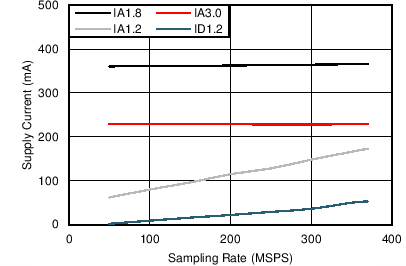
| IA3.0 | VA3.0 supply current consumption | Normal operation, single data lane per channel | 230 | mA | |||
| Normal operation, dual data lane per channel | 255 | ||||||
| Power down mode | 8.7 | ||||||
| IA1.8 | VA1.8 supply current consumption | Normal operation | 360 | mA | |||
| Power down mode | 3.6 | ||||||
| IA1.2 | VA1.2 supply current consumption | Normal operation | 172 | mA | |||
| Power down mode | 3.3 | ||||||
| ID1.2 | VD1.2 supply current consumption | Normal operation | 52 | mA | |||
| Power down mode | 3.3 | ||||||
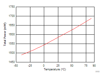
| PT | Total power consumption of the VA3.0 , VA1.8 , VA1.2 , VD1.2 supplies |
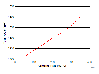
Normal operation, single serial lane per channel | TA = 25°C | 1607 | mW | ||
| TA = TMIN to TMAX | 1800 | ||||||
| Power consumption during power-down state, external clock active | 30 | ||||||
| Power consumption during sleep state, external clock active | 30 | ||||||
| VBP2.5 | Voltage at the BP2.5 pin | 2.65 | V | ||||
| Supply sensitivity to noise Power of spectral spur resulting from a 100-mV sinusoidal signal modulating a supply at 500 kHz. Analog input is a –3 dBFS 150-MHz single tone. In all cases, the spur appears as part of a pair symmetric about the fundamental that scales proportionally with the fundamental amplitude. |
dBFS | ||||||
| VA3.0 | –72.5 | ||||||
| VA1.8 | –58.0 | ||||||
| VA1.2 | –37.7 | ||||||
| VD1.2 | –78 | ||||||
(1) Power values indicate consumption during normal conversion assuming JESD204 link establishment
6.7 Analog Interface Electrical Characteristics
Unless otherwise noted, these specifications apply for VA3.0 = 3 V; VA1.8 = 1.8 V; VA1.2 = VD1.2 = 1.2 V; FCLKIN = FS = 370 MSPS; external differential resistive termination at ADC input is 66 Ω. Typical values are at TA = 25°C.| PARAMETER | DESCRIPTION AND TEST CONDITIONS | MIN | TYP | MAX | UNIT | ||
|---|---|---|---|---|---|---|---|
| FSR | Full scale range Differential peak-to-peak |
1.7 | Vpp | ||||
| GVAR | Gain variation Variation of input voltage to output code gain between different parts, part-to-part or channel-to-channel |
±0.07 | dB | ||||
| VOFF | Input referred voltage offset | ±13 | mV | ||||
| BW3dB | 3-dB bandwidth Frequency at which the voltage input to digital output response deviates by 3 dB compared to low frequencies for a low impedance differential signal applied at the input pins. Includes 0.5-nH parasitic inductance in series with each pin of the differential analog input. |
800 | MHz | ||||
| RIN | Input termination resistance Differential |
200 | Ω | ||||
| CIN | Input capacitance, differential | 3.7 | pF | ||||
| VCMA, VCMB | Input common mode voltage reference voltage at the VCMA or VCMB pins Varies with temperature |
1.6 | V | ||||
| IVCM | Input common mode voltage reference current sourcing or sinking on VCMA or VCMB pins | 1 | mA | ||||
| VCM-OFF | Input common mode voltage offset range Allowable difference between the common mode applied to the analog input of a particular channel and the bias voltage at the respective common mode VCM bias pin (VCMA or VCMB) |
±50 | mV | ||||
6.8 CLKIN, SYSREF, SYNCb Interface Electrical Characteristics
Unless otherwise noted, these specifications apply for VA3.0 = 3 V; VA1.8 = 1.8 V; VA1.2 = VD1.2 = 1.2 V; FCLKIN = FS = 370 MSPS. Typical values are at TA = 25°C.| PARAMETER | DESCRIPTION AND TEST CONDITIONS | MIN | TYP | MAX | UNIT | |
|---|---|---|---|---|---|---|
| DIGITAL INPUT CHARACTERISTICS (CLKIN) | ||||||
| VID | Input differential voltage(1)(3)
Differential peak voltage |
250 | 1000 | mV | ||
| dVSS/dt | Recommended minimum edge slew rate at the zero crossing(1)
|
2 | 5 | V/ns | ||
| VIS-BIAS | Input offset voltage internal bias (1)
Internally biased |
0.5 | V | |||
| VIS-IN | Externally applied input offset voltage(3)
Allowable common mode voltage range for DC coupled interfaces |
0.4 | 0.5 | 0.6 | V | |
| Zrdiff | Differential termination resistance at DC(2) | 130 | Ω | |||
| Ztt | Common-mode bias source impedance(2) | 11 | kΩ | |||
| CT | Differential termination capacitance | 1.5 | pF | |||
| DIGITAL INPUT CHARACTERISTICS (SYSREF) | ||||||
| VID | Input differential voltage (1)(3)
Differential peak voltage |
250 | 1000 | mV | ||
| VIS-BIAS | Input offset voltage bias (1)
Internally biased |
0.5 | V | |||
| VIS-IN | Externally applied input offset voltage(3)
Allowable common mode voltage range for DC coupled interfaces |
0.4 | 0.5 | 0.6 | V | |
| Zrdiff | Differential termination resistance at DC(2) | 2 | kΩ | |||
| Ztt | Common-mode bias source impedance(2) | 11 | kΩ | |||
| CT | Differential termination capacitance(2) | 0.8 | pF | |||
| DIGITAL INPUT CHARACTERISTICS (SYNCb) | ||||||
| VID | Input differential voltage (1)(3)
Differential peak voltage |
350 | mV | |||
| VIS-IN | Externally applied input offset voltage(1)(3) | 0.5 | 1.2 | 2 | V | |
| Zrdiff | Differential termination resistance(2) | 100 | Ω | |||
| CT | Differential termination capacitance(2) | 1 | pF | |||
(1) Specification applies to the electrical level diagram of Figure 1
(2) Specification applies to the electrical circuit diagram of Figure 2
(3) The voltage present at the pins should not exceed Absolute Maximum limits
 Figure 1. Electrical Level Diagram for Differential Input Signals
 Figure 2. Simplified Electrical Circuit Diagram for Differential Input Signals
6.9 Serial Data Output Interface Electrical Characteristics
Unless otherwise noted, these specifications apply for VA3.0 = 3 V; VA1.8 = 1.8 V; VA1.2 = VD1.2 = 1.2 V; FCLKIN = FS = 370 MSPS. Typical values are at TA = 25°C.| PARAMETER | DESCRIPTION AND TEST CONDITIONS | MIN | TYP | MAX | UNIT | |
|---|---|---|---|---|---|---|
| SERIAL LANE OUTPUT CHARACTERISTICS (SA0, SA1, SB0, SB1) | ||||||
| VOD | Output differential voltage(1)
Differential peak-peak values. Assumes ideal 100-Ω load. De-emphasis disabled. Configurable via SPI |
580 680 760 860 960 1060 1140 1240 |
mV | |||
| Zddiff | Differential output impedance at DC(2) | 100 | Ω | |||
| RLddiff | Differential output return loss magnitude Relative to 100 Ω; For frequencies up to 5.5 GHz |
–11 | dB | |||
| Rdeemp | Transmitter de-emphasis values VOD configured to default value. |
0 0.4 1.2 2.1 2.8 3.8 4.8 6.8 |
dB | |||
(1) Specification applies to the electrical level diagram of Figure 3
(2) Specification applies to the electrical circuit diagram of Figure 4
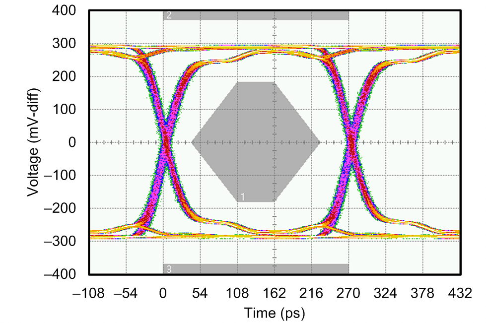
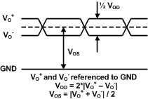 Figure 3. Electrical Level Diagram for Differential Output Signals
 Figure 4. Electrical Circuit Diagram for Differential Output Signals
6.10 Digital Input Electrical Interface Characteristics
Unless otherwise noted, these specifications apply for VA3.0= 3 V; VA1.8 = 1.8 V; VA1.2 = VD1.2 = 1.2 V; FCLKIN = FS = 370 MSPS. Typical values are at TA = 25°C.| PARAMETER | DESCRIPTION AND TEST CONDITIONS | MIN | TYP | MAX | UNIT | |
|---|---|---|---|---|---|---|
| DIGITAL INPUT CHARACTERISTICS (SDI, SCLK, CSB) | ||||||
| VIH | Logical 1 input voltage(1)
Inputs are compatible with 1.2-V up to 3.0-V logic. |
0.9 | V | |||
| VIL | Logical 0 input voltage(1) | 0.3 | V | |||
| IIN0 | Logic low input current | 0.5 | uA | |||
| IIN1 | Logic high input current | 0.5 | uA | |||
| CIN | Input capacitance | 2 | pF | |||
| DIGITAL OUTPUT CHARACTERISTICS (SDO) | ||||||
| VOH | Logical 1 output voltage(1)(2)
VSPI = 1.2, 1.8, 2.5, or 3 V ; Configurable via SPI |
VSPI – 0.3 | VSPI(2) | V | ||
| VOL | Logical 0 output voltage(1)(2) | 0 | 0.3 | V | ||
| +ISC | Logic high short circuit current | 9 | mA | |||
| –ISC | Logic low short circuit current | –10 | mA | |||
| DIGITAL OUTPUT CHARACTERISTICS (OVRA/TRIGRDY, OVRB) | ||||||
| VOH | Logical 1 output voltage(1) | 1.5 | 1.8 | V | ||
| VOL | Logical 0 output voltage(1) | 0 | 0.3 | V | ||
| +ISC | Logic high short circuit current | 17.7 | mA | |||
| –ISC | Logic low short circuit current | –15 | mA | |||
| DIGITAL INPUT CHARACTERISTICS (TRIGGER) | ||||||
| VIH | Logical 1 input voltage(1) | 1.5 | V | |||
| VIL | Logical 0 input voltage(1) | 0.3 | V | |||
| IIN0 | Logic low input current | 0.5 | uA | |||
| IIN1 | Logic high input current | 0.5 | uA | |||
| CIN | Input capacitance | 3 | pF | |||
(1) Specification applies to the electrical level diagram of Figure 5.
(2) The SPI_CFG register must be changed to a supported output logic level after power up and before a read command is executed. Until that time, the output voltage on SDO may be as high as the VA3.0 supply during a read command. The SDO output is high-Z at all times except during a read command.
 Figure 5. Electrical Level Diagram for Single-ended Digital Inputs and Outputs
6.11 Timing Requirements
Unless otherwise noted, these specifications apply for VA3.0= 3 V; VA1.8 = 1.8 V; VA1.2 = VD1.2 = 1.2 V; FCLKIN = FS = 370 MSPS. Typical values are at TA = 25°C.| PARAMETER | DESCRIPTION | MIN | TYP | MAX | UNIT | |
|---|---|---|---|---|---|---|
| ADC SAMPLING INSTANT TIMING CHARACTERISTICS | ||||||
| FS | Sampling rate Equal to FCLKIN / CLKDIV |
50 | 370 | MSPS | ||
| FCLKIN | Input Clock Frequency at CLKIN Inputs | MHz | ||||
| CLKDIV = 1 | 50 | 370 | ||||
| CLKDIV = 2 | 100 | 740 | ||||
| CLKDIV = 4 | 200 | 1480 | ||||
| CLKDIV = 8 | 400 | 2000 | ||||
| tLAT-ADC | ADC core latency Delay from a reference sampling instant to the boundary of the internal LMFC where the reference sample is the first sample of the next transmitted multi-frame. Coarse sampling phase adjust disabled. In this device, the frame clock period is equal to the sampling clock period. |
12.5 | Frame clock cycles | |||
| tJ | Additive sampling aperture jitter Depends on input CLKIN differential edge rate at the zero crossing, dVSS/dt. Tested with 5 V/ns edge rate. |
fs | ||||
| CLKDIV = 1 | 70 | |||||
| CLKDIV = 2, 4, coarse phase disabled | 80 | |||||
| CLKDIV = 4, coarse phase enabled. Typical worst-case value across all coarse phase configuration possibilities. | 85 | |||||
| OVER-RANGE INTERFACE TIMING CHARACTERISTICS (OVRA, OVRB) | ||||||
| tODH | OVR assertion delay Delay between an over-range value sampled and OVR asserted; Coarse clock phase adjust disabled. |
7.5 | Frame clock cycles | |||
| tODL | OVR de-assertion delay Delay between first under-range value sampled until OVR de-assertion; Configurable via SPI. |
tODH + 0 | tODH + 15 | Frame clock cycles | ||
| SYSREF TIMING CHARACTERISTICS | ||||||
| tPH-SYS | SYSREF assertion duration Required duration of SYSREF assertion after rising edge event |
2 | Frame clock cycles | |||
| tPL-SYS | SYSREF de-assertion duration Required duration of SYSREF de-assertion after falling edge event |
2 | Frame clock cycles | |||
| tS-SYS | SYSREF setup time Relative to CLKIN rising edge |
320 | ps | |||
| tH-SYS | SYSREF hold time Relative to CLKIN rising edge |
80 | ps | |||
| JESD204B INTERFACE LINK TIMING CHARACTERISTICS | ||||||
| tD-LMFC | SYSREF to LMFC delay Functional delay between SYSREF assertion latched and LMFC frame boundary. Depends on CLKDIV setting. |
CLKIN cycles (Frame clock cycles) |
||||
| CLKDIV = 1 | 3.5 (3.5) |
|||||
| CLKDIV = 2 | 8 (4) |
|||||
| CLKDIV = 4 | 15 (3.75) |
|||||
| CLKDIV = 8 | 29 (3.625) |
|||||
| tD-K28 | LMFC to K28.5 delay Functional delay between the start of the first K28.5 frame during Code Group Synchronization at the serial output and the preceding LMFC frame boundary. |
5 | 6 | 7 | Frame clock cycles | |
| tD-ILA | LMFC to ILA delay Functional delay between the start of the first ILA frame during Initial Lane Synchronization at the serial output and the preceding LMFC frame boundary |
5 | 6 | 7 | ||
| tD-DATA | LMFC to valid data delay Functional delay between the start of the first valid data frame at the serial output and the preceding LMFC frame boundary. |
5 | 6 | 7 | ||
| tS-SYNCb-F | SYNCb setup time Required SYNCb setup time relative to the internal LMFC boundary. |
3 | Frame clock cycles | |||
| tH-SYNCb-F | SYNCb hold time Required SYNCb hold time relative to the internal LMFC boundary . |
0 | ||||
| tH-SYNCb | SYNCb assertion hold time Required SYNCb hold time after assertion before de-assertion to initiate a link re-synchronization. |
4 | ||||
| tILA | ILA duration Duration of the ILA sequence . |
4 | Multi-frame clock cycles | |||
| SERIAL OUTPUT DATA TIMING CHARACTERISTICS | ||||||
| FSR | Serial bit rate Single- or dual-lane mode |
1 | 7.4 | Gb/s | ||
| UI | Unit Interval 7.4 Gb/s Data Rate |
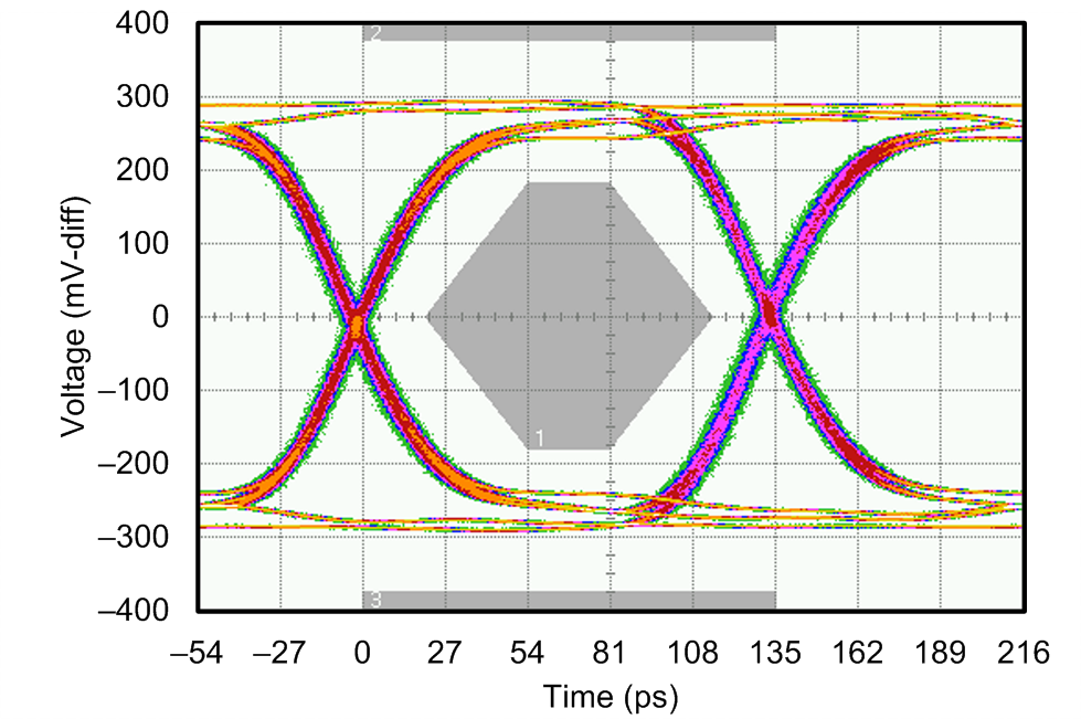
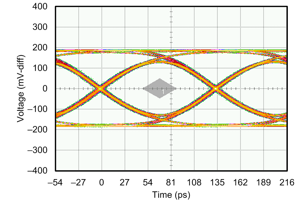
135.1 | ps | |||
| DJ | Deterministic jitter Includes periodic jitter (PJ), data dependent jitter (DDJ), duty cycle distortion (DCD), and inter-symbol interference (ISI); 7.4 Gb/s data rate. |
0.047 (6.33) |
p-p UI (p-p ps) |
|||
| RJ | Random jitter Assumes BER of 1e-15 (Q = 15.88); 7.4 Gb/s data rate |
0.156 (1.35) |
p-p UI (rms ps) |
|||
| TJ | Total jitter Sum of DJ and RJ. Assumes BER of 1e-15 (Q = 15.88); 7.4 Gb/s data rate. |
0.206 (27.77) |
p-p UI (p-p ps) |
|||
| SPI BUS TIMING CHARACTERISTICS(1) | ||||||
| ƒSCLK | Serial clock frequency fSCLK = 1 / tP |
20 | MHz | |||
| tPH | SCLK pulse width – high % of SCLK period |
25% | 75% | |||
| tPL | SCLK pulse width – low % of SCLK period |
25% | 75% | |||
| tSSU | SDI input data setup time | 5 | ns | |||
| tSH | SDI input data hold time | 5 | ns | |||
| tODZ | SDO output data driven-to-3-state time | 25 | ns | |||
| tOZD | SDO output data 3-state-to-driven time | 25 | ns | |||
| tOD | SDO output data delay time | 30 | ns | |||
| tCSS | CSB setup time | 5 | ns | |||
| tCSH | CSB hold time | 5 | ns | |||
| tIAG | Inter-access gap Minimum time CSB must be de-asserted between accesses |
5 | ns | |||
(1) All timing specifications for the SPI given for VSPI = 1.8-V logic levels and a 5-pF capacitive load on the SDO pin. Timing specification may require larger margins for VSPI= 1.2 V.
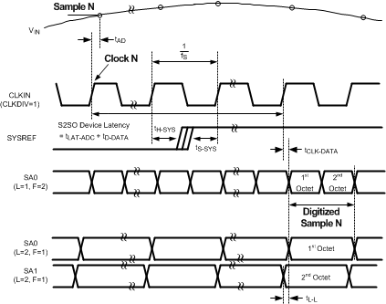 Figure 6. Sample to Data Timing Diagram
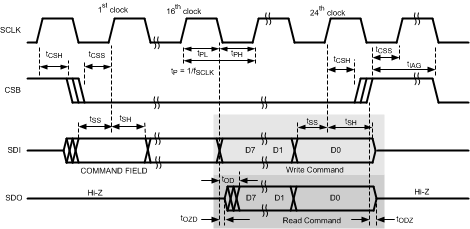 Figure 7. SPI Timing Diagram
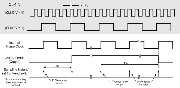 Figure 8. Over-Range Timing Diagram
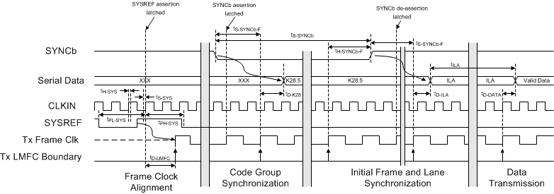 Figure 9. JESD204B Interface Link Initialization Timing Diagram
For more information, see Functional Block Diagram.
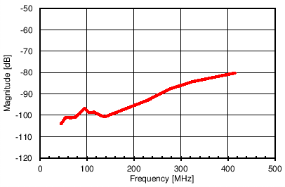
6.12 Typical Characteristics
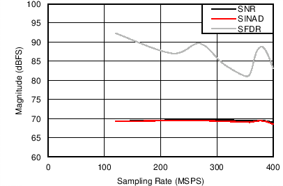
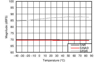
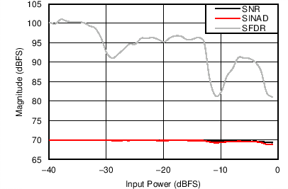
Unless otherwise noted, these specifications apply for VA3.0 = 3 V; VA1.8 = 1.8 V; VA1.2 = VD1.2 = 1.2 V; FCLKIN = FS = 370 MSPS; 150-MHz input frequency; –3-dBFS input power. Typical values are at TA = 25°C.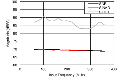
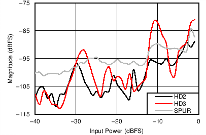
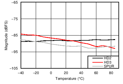
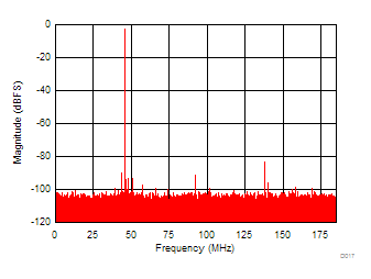
| SNR = 68.49 dBFS | SFDR = 83.21 dBFS | |
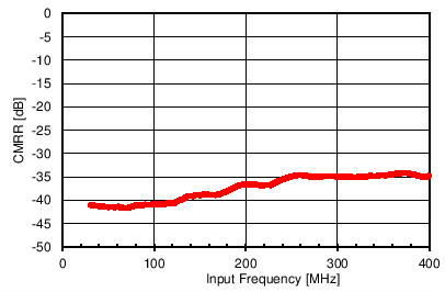
–24-dBm Input)
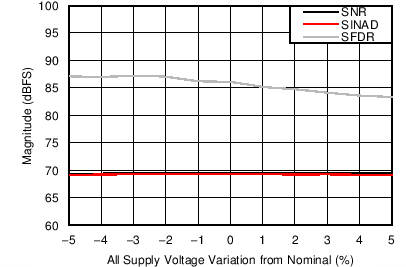
| Nominal Supplies: | VA3.0 = 3.0 V | VA1.2 = VD1.2 = 1.2 V |
| VA1.8 = 1.8 V |
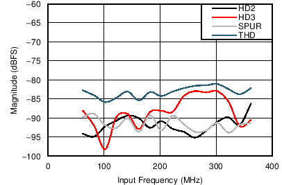
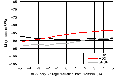
| Nominal Supplies: | VA3.0 = 3.0 V | VA1.2 = VD1.2 = 1.2 V |
| VA1.8 = 1.8 V |
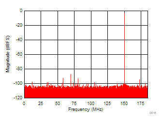
| SNR = 69.5 dBFS | SFDR = 87.0 dBFS |
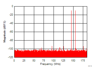
| SNR = 69.5 dBFS | SFDR = 94 dBFS | IMD3 = –100 dBFS |
145 and 155 MHz)
