ZHCSE48B September 2015 – January 2019 ADC31JB68
PRODUCTION DATA.
- 1 特性
- 2 应用
- 3 说明
- 4 修订历史记录
- 5 Pin Configuration and Functions
- 6 Specifications
- 7 Parameter Measurement Information
-
8 Detailed Description
- 8.1 Overview
- 8.2 Functional Block Diagram
- 8.3
Feature Description
- 8.3.1 Analog Inputs and Input Buffer
- 8.3.2 Amplitude and Phase Imbalance Correction
- 8.3.3 Over-Range Detection
- 8.3.4 Input Clock Divider
- 8.3.5 SYSREF Detection Gate
- 8.3.6 Serial Differential Output Drivers
- 8.3.7 ADC Core Calibration
- 8.3.8 Data Format
- 8.3.9 JESD204B Supported Features
- 8.3.10 JESD204B Interface
- 8.3.11 Transport Layer Configuration
- 8.3.12 Test Pattern Sequences
- 8.3.13 JESD204B Link Initialization
- 8.3.14 SPI
- 8.4 Device Functional Modes
- 8.5
Register Map
- 8.5.1
Register Descriptions
- 8.5.1.1 CONFIG_A (address = 0x0000) [reset = 0x3C]
- 8.5.1.2 DEVICE CONFIG (address = 0x0002) [reset = 0x00]
- 8.5.1.3 CHIP_TYPE (address = 0x0003 ) [reset = 0x03]
- 8.5.1.4 CHIP_ID (address = 0x0005, 0x0004) [reset = 0x00, 0x1B]
- 8.5.1.5 CHIP_VERSION (address =0x0006) [reset = 0x00]
- 8.5.1.6 VENDOR_ID (address = 0x000D, 0x000C) [reset = 0x04, 0x51]
- 8.5.1.7 SPI_CFG (address = 0x0010 ) [reset = 0x01]
- 8.5.1.8 OM1 (Operational Mode 1) (address = 0x0012) [reset = 0xC1]
- 8.5.1.9 OM2 (Operational Mode 2) (address = 0x0013) [reset = 0x20]
- 8.5.1.10 IMB_ADJ (Imbalance Adjust) (address = 0x0014) [reset = 0x00]
- 8.5.1.11 OVR_EN (Over-Range Enable) (address = 0x003A) [reset = 0x00]
- 8.5.1.12 OVR_HOLD (Over-Range Hold) (address = 0x003B) [reset = 0x00]
- 8.5.1.13 OVR_TH (Over-Range Threshold) (address = 0x003C) [reset = 0x00]
- 8.5.1.14 DC_MODE (DC Offset Correction Mode) (address = 0x003D) [reset = 0x00]
- 8.5.1.15 SER_CFG (Serial Lane Transmitter Configuration) (address = 0x0047) [reset = 0x00]
- 8.5.1.16 JESD_CTRL1 (JESD Configuration Control 1) (address = 0x0060) [reset = 0x7F]
- 8.5.1.17 JESD_CTRL2 (JESD Configuration Control 2) (address = 0x0061) [reset = 0x00]
- 8.5.1.18 JESD_RSTEP (JESD Ramp Pattern Step) (address = 0x0063, 0x0062) [reset = 0x00, 0x01]
- 8.5.1.19 SER_INV (Serial Lane Inversion Control) (address = 0x0064) [reset = 0x00]
- 8.5.1.20 JESD_STATUS (JESD Link Status) (address = 0x006C) [reset = N/A]
- 8.5.1
Register Descriptions
- 9 Application and Implementation
- 10Power Supply Recommendations
- 11Layout
- 12器件和文档支持
- 13机械、封装和可订购信息
11.1 Layout Guidelines
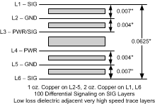
The design of the PCB is critical to achieve the full performance of the ADC31JB68 device. Defining the PCB stackup should be the first step in the board design. Experience has shown that at least 6 layers are required to adequately route all required signals to and from the device. Each signal routing layer must have an adjacent solid ground plane to control signal return paths to have minimal loop areas and to achieve controlled impedances for microstrip and stripline routing. Power planes must also have adjacent solid ground planes to control supply return paths. Minimizing the spacing between supply and ground planes improves performance by increasing the distributed decoupling. A recommended stack-up for a 6-layer board design is shown in Figure 80.
Although the ADC31JB68 device consists of both analog and digital circuitry, TI highly recommends solid ground planes that encompass the device and its input and output signal paths. TI does not recommend split ground planes that divide the analog and digital portions of the device. Split ground planes may improve performance if a nearby, noisy, digital device is corrupting the ground reference of the analog signal path. When split ground planes are employed, one must carefully control the supply return paths and keep the paths on top of their respective reference planes.
Quality analog input signal and clock signal path layout is required for full dynamic performance. Symmetry of the differential signal paths and discrete components in the path is mandatory and symmetrical shunt-oriented components should have a common grounding via. The high frequency requirements of the input and clock signal paths necessitate using differential routing with controlled impedances and minimizing signal path stubs (including vias) when possible.
Coupling onto or between the clock and input signal paths must be avoided using any isolation techniques available including distance isolation, orientation planning to prevent field coupling of components like inductors and transformers, and providing well coupled reference planes. Via stitching around the clock signal path and the input analog signal path provides a quiet ground reference for the critical signal paths and reduces noise coupling onto these paths. Sensitive signal traces must not cross other signal traces or power routing on adjacent PCB layers, rather a ground plane should separate the traces. If necessary, the traces should cross at 90° angles to minimize crosstalk.
The substrate dielectric materials of the PCB are largely influenced by the speed and length of the high speed serial lanes. The affordable and common FR4 variety may not offer the consistency or low loss to support the highest speed transmission (5 Gb/s) and long lengths (> 8 inch). Although the VOD and DEM features are available to improve the signal integrity of the serial lanes, some of the highest performing applications may still require special dielectric materials.
Coupling of ambient signals into the signal path is reduced by providing quiet, close reference planes and by maintaining signal path symmetry to ensure the coupled noise is common-mode. Faraday caging may be used in very noisy environments and high dynamic range applications to isolate the signal path.
 Figure 80. Recommended PCB Layer Stack-Up for a Six-Layer Board