ZHCSE48B September 2015 – January 2019 ADC31JB68
PRODUCTION DATA.
- 1 特性
- 2 应用
- 3 说明
- 4 修订历史记录
- 5 Pin Configuration and Functions
- 6 Specifications
- 7 Parameter Measurement Information
-
8 Detailed Description
- 8.1 Overview
- 8.2 Functional Block Diagram
- 8.3
Feature Description
- 8.3.1 Analog Inputs and Input Buffer
- 8.3.2 Amplitude and Phase Imbalance Correction
- 8.3.3 Over-Range Detection
- 8.3.4 Input Clock Divider
- 8.3.5 SYSREF Detection Gate
- 8.3.6 Serial Differential Output Drivers
- 8.3.7 ADC Core Calibration
- 8.3.8 Data Format
- 8.3.9 JESD204B Supported Features
- 8.3.10 JESD204B Interface
- 8.3.11 Transport Layer Configuration
- 8.3.12 Test Pattern Sequences
- 8.3.13 JESD204B Link Initialization
- 8.3.14 SPI
- 8.4 Device Functional Modes
- 8.5
Register Map
- 8.5.1
Register Descriptions
- 8.5.1.1 CONFIG_A (address = 0x0000) [reset = 0x3C]
- 8.5.1.2 DEVICE CONFIG (address = 0x0002) [reset = 0x00]
- 8.5.1.3 CHIP_TYPE (address = 0x0003 ) [reset = 0x03]
- 8.5.1.4 CHIP_ID (address = 0x0005, 0x0004) [reset = 0x00, 0x1B]
- 8.5.1.5 CHIP_VERSION (address =0x0006) [reset = 0x00]
- 8.5.1.6 VENDOR_ID (address = 0x000D, 0x000C) [reset = 0x04, 0x51]
- 8.5.1.7 SPI_CFG (address = 0x0010 ) [reset = 0x01]
- 8.5.1.8 OM1 (Operational Mode 1) (address = 0x0012) [reset = 0xC1]
- 8.5.1.9 OM2 (Operational Mode 2) (address = 0x0013) [reset = 0x20]
- 8.5.1.10 IMB_ADJ (Imbalance Adjust) (address = 0x0014) [reset = 0x00]
- 8.5.1.11 OVR_EN (Over-Range Enable) (address = 0x003A) [reset = 0x00]
- 8.5.1.12 OVR_HOLD (Over-Range Hold) (address = 0x003B) [reset = 0x00]
- 8.5.1.13 OVR_TH (Over-Range Threshold) (address = 0x003C) [reset = 0x00]
- 8.5.1.14 DC_MODE (DC Offset Correction Mode) (address = 0x003D) [reset = 0x00]
- 8.5.1.15 SER_CFG (Serial Lane Transmitter Configuration) (address = 0x0047) [reset = 0x00]
- 8.5.1.16 JESD_CTRL1 (JESD Configuration Control 1) (address = 0x0060) [reset = 0x7F]
- 8.5.1.17 JESD_CTRL2 (JESD Configuration Control 2) (address = 0x0061) [reset = 0x00]
- 8.5.1.18 JESD_RSTEP (JESD Ramp Pattern Step) (address = 0x0063, 0x0062) [reset = 0x00, 0x01]
- 8.5.1.19 SER_INV (Serial Lane Inversion Control) (address = 0x0064) [reset = 0x00]
- 8.5.1.20 JESD_STATUS (JESD Link Status) (address = 0x006C) [reset = N/A]
- 8.5.1
Register Descriptions
- 9 Application and Implementation
- 10Power Supply Recommendations
- 11Layout
- 12器件和文档支持
- 13机械、封装和可订购信息
8.3.13.2 Code Group Synchronization
Code Group Synchronization is initiated when the receiver sends a synchronization request by asserting the SYNCb input of the ADC31JB68 device to a logic low state (SYNCb+ < SYNCb–). After the SYNCb assertion is detected, the ADC31JB68 device outputs K28.5 symbols on all serial lanes. These symbols are used by the receiver to synchronize and time align its clock and data recovery (CDR) block to the known symbols. The SYNCb signal must be asserted for at least 4 frame clock cycles otherwise the event is ignored by the ADC31JB68 device. Code group synchronization is completed when the receiver de-asserts the SYNCb signal to a logic high state.
After the ADC31JB68 detects a de-assertion of its SYNCb input, the Initial Lane Synchronization step begins on the following LMFC boundary. The ADC31JB68 device outputs 4 multi-frames of information that compose the ILA sequence. This sequence contains information about the data transmitted on the link. The initial lane synchronization step and link initialization conclude when the ILA is finished and immediately transitions into Data Transmission. During data transmission, valid sampled data is transmitted across the link until the link is broken.
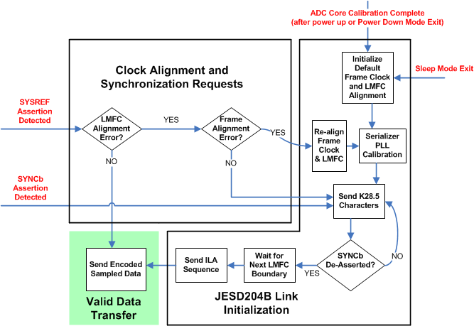
 Figure 36. Device Start-Up and JESD204B Link Synchronization Flow Chart
 The flowchart in Figure 36 describes how the ADC31JB68 device initializes the JESD204B link and reacts to changes in the link. After the ADC core calibration is finished, the ADC31JB68 device begins with PLL calibration and link initialization using a default frame clock and LMFC alignment by sending K28.5 characters. PLL calibration requires approximately 153×103 sampling clock cycles. If SYNCb is not asserted, then the device immediately advances to the ILA sequence at the next LMFC boundary. If SYNCb is asserted, then the device continues to output K28.5 characters until SYNCb is de-asserted.
When a SYSREF rising edge event is detected, then the ADC31JB68 device compares the SYSREF event to the current alignment of the LMFC. If the SYSREF event is aligned to the current LMFC alignment, then no action is taken and the device continues to output data. If misalignment is detected, then the SYSREF event is compared to the frame clock. If misalignment of the frame clock is also detected, then the clocks are re-aligned and the link is reinitialized. If the frame clock is not misaligned, then the frame clock alignment is not updated. In the cases that a SYSREF event causes a link re-initialization, the ADC31JB68 device begins sending K28.5 characters without a SYNCb assertion and immediately transitions to the ILA sequence on the next LMFC boundary unless the SYNCb signal is asserted. Anytime the frame clock and LMFC are re-aligned, the serializer PLL must calibrate before code group synchronization begins. SYSREF events must not occur during ADC31JB68 device power-up, ADC calibration, or PLL calibration. The JESD_STATUS register is available to check the status of the ADC31JB68 device and the JESD204B link.
If a SYNCb assertion is detected for at least 4 frame clock cycles, the ADC31JB68 device immediately breaks the link and sends K28.5 characters until the SYNCb signal is de-asserted.
When exiting sleep mode, the frame clock and LMFC are started with a default (unknown) phase alignment, PLL calibration is performed, and the device immediately transitions into sending K28.5 characters.