ZHCSE48B September 2015 – January 2019 ADC31JB68
PRODUCTION DATA.
- 1 特性
- 2 应用
- 3 说明
- 4 修订历史记录
- 5 Pin Configuration and Functions
- 6 Specifications
- 7 Parameter Measurement Information
-
8 Detailed Description
- 8.1 Overview
- 8.2 Functional Block Diagram
- 8.3
Feature Description
- 8.3.1 Analog Inputs and Input Buffer
- 8.3.2 Amplitude and Phase Imbalance Correction
- 8.3.3 Over-Range Detection
- 8.3.4 Input Clock Divider
- 8.3.5 SYSREF Detection Gate
- 8.3.6 Serial Differential Output Drivers
- 8.3.7 ADC Core Calibration
- 8.3.8 Data Format
- 8.3.9 JESD204B Supported Features
- 8.3.10 JESD204B Interface
- 8.3.11 Transport Layer Configuration
- 8.3.12 Test Pattern Sequences
- 8.3.13 JESD204B Link Initialization
- 8.3.14 SPI
- 8.4 Device Functional Modes
- 8.5
Register Map
- 8.5.1
Register Descriptions
- 8.5.1.1 CONFIG_A (address = 0x0000) [reset = 0x3C]
- 8.5.1.2 DEVICE CONFIG (address = 0x0002) [reset = 0x00]
- 8.5.1.3 CHIP_TYPE (address = 0x0003 ) [reset = 0x03]
- 8.5.1.4 CHIP_ID (address = 0x0005, 0x0004) [reset = 0x00, 0x1B]
- 8.5.1.5 CHIP_VERSION (address =0x0006) [reset = 0x00]
- 8.5.1.6 VENDOR_ID (address = 0x000D, 0x000C) [reset = 0x04, 0x51]
- 8.5.1.7 SPI_CFG (address = 0x0010 ) [reset = 0x01]
- 8.5.1.8 OM1 (Operational Mode 1) (address = 0x0012) [reset = 0xC1]
- 8.5.1.9 OM2 (Operational Mode 2) (address = 0x0013) [reset = 0x20]
- 8.5.1.10 IMB_ADJ (Imbalance Adjust) (address = 0x0014) [reset = 0x00]
- 8.5.1.11 OVR_EN (Over-Range Enable) (address = 0x003A) [reset = 0x00]
- 8.5.1.12 OVR_HOLD (Over-Range Hold) (address = 0x003B) [reset = 0x00]
- 8.5.1.13 OVR_TH (Over-Range Threshold) (address = 0x003C) [reset = 0x00]
- 8.5.1.14 DC_MODE (DC Offset Correction Mode) (address = 0x003D) [reset = 0x00]
- 8.5.1.15 SER_CFG (Serial Lane Transmitter Configuration) (address = 0x0047) [reset = 0x00]
- 8.5.1.16 JESD_CTRL1 (JESD Configuration Control 1) (address = 0x0060) [reset = 0x7F]
- 8.5.1.17 JESD_CTRL2 (JESD Configuration Control 2) (address = 0x0061) [reset = 0x00]
- 8.5.1.18 JESD_RSTEP (JESD Ramp Pattern Step) (address = 0x0063, 0x0062) [reset = 0x00, 0x01]
- 8.5.1.19 SER_INV (Serial Lane Inversion Control) (address = 0x0064) [reset = 0x00]
- 8.5.1.20 JESD_STATUS (JESD Link Status) (address = 0x006C) [reset = N/A]
- 8.5.1
Register Descriptions
- 9 Application and Implementation
- 10Power Supply Recommendations
- 11Layout
- 12器件和文档支持
- 13机械、封装和可订购信息
5 Pin Configuration and Functions
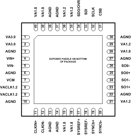
The ADC31JB68 is packaged in a 40-pin QFN package (6 x 6 x 0.8, 0.5 mm pin-pitch) with a bottom-side exposed paddle.
RTA Package
40 PIN (WQFN)
Top View
Pin Functions
| PIN | TYPE or DIAGRAM | DESCRIPTION | ||||
|---|---|---|---|---|---|---|
| NAME | NO. | |||||
| INPUT/REFERENCE | ||||||
| VIN+
VIN– |
4, 5 |
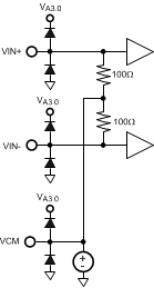 |
Differential analog input pins.
The differential full-scale signal level is 1.7 Vpp. Each input pin is terminated to the internal 1.6V common-mode reference with a 100 Ω resistor for a 200 Ω total differential termination. |
|||
| VCM | 7 | Input Interface Common mode voltage.
This pin must be bypassed to AGND with a low ESL (equivalent series inductance) 0.1 µF capacitor that is placed as close to the pin as possible to minimize stray inductance. A 10 µF capacitor should also be placed in parallel. It is recommended to use VCM to provide the common mode voltage for the differential analog inputs. The input common-mode bias is provided internally for the ADC input, therefore external use of VCM is recommended but not strictly required. The recommended decoupling is always required. |
||||
| CLOCK/SYNC | ||||||
| CLKIN+
CLKIN– |
11, 12 |
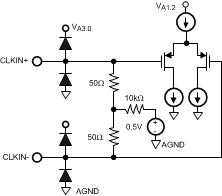 |
Differential device clock input pins.
AC coupling is recommended for coupling the clock input to these pins. DC biasing of the clock receiver is provided internally. Each pin is internally terminated to the 500mV DC bias with 50 Ω resistor for a 100 Ω total internal differential termination resistor. Sampling occurs on the falling edge of the differential signal (CLKIN+) − (CLKIN-). |
|||
| SYSREF+,
SYSREF– |
17, 18 | 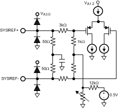 |
Differential SYSREF signal input pins.
Each pin is internally terminated to the DC bias with a large resistor. An internal 100 Ω differential termination is provided therefore an external termination is not required. Additional resistive components in the input structure give the SYSREF input a wide input common mode range. |
|||
| SYNCb+
SYNCb– |
19, 20 | 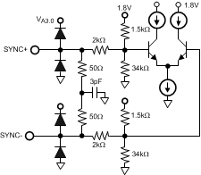 |
Differential SYNCb signal input pins. | |||
| DC coupling is required for coupling the SYNCb signal to these pins. Each pin is internally terminated to the DC bias with a large resistor. An internal 100 Ω differential termination is provided therefore an external termination is not required. Additional resistive components in the input structure give the SYNCb input a wide input common mode range. The SYNCb signal is active low and is therefore asserted when the voltage at SYNCb+ is less than at SYNCb–. | ||||||
| SERIAL INTERFACE (SPI) | ||||||
| SCLK | 32 |  |
SPI Interface Serial Clock pin.
Serial data is shifted into and out of the device synchronous with this clock signal. Compatible with 1.2–3.0V CMOS logic levels. |
|||
| CSB | 31 | SPI Interface Chip Select pin.
When this signal is asserted, SCLK is used to clock input serial data on the SDI pin or output serial data on the SDO pin. When this signal is de-asserted, the SDO pin is high impedance and the input data is ignored. Active low. A 1kΩ pull-up resistor to the VA1.8 supply is recommended to prevent undesired activation of the SPI bus. Compatible with 1.2–3.0V CMOS logic levels. |
||||
| SDI | 33 | SPI Interface Data Input pin.
Serial data is shifted into the device on this pin while the CSB signal is asserted. Compatible with 1.2-3.0V CMOS logic levels. |
||||
| SDO/OVR | 34 | 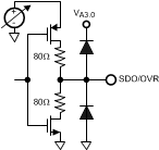 |
SPI Data Output and Over-Range pin.
Dual mode pin. When configured as SDO, serial data of the SPI is shifted out of the device on this pin while CSB is asserted. When configured as OVR, the over-range signal is output. Pin mode configurable via the SPI. Output voltage is configurable to 1.2V, 1.8V, or 3.0V CMOS logic levels via the SPI. Default configuration outputs the SDO at a 1.8V logic level. |
|||
| DIGITAL OUTPUT INTERFACE | ||||||
| SO0+, SO0–,
SO1+, SO1– |
25, 26,
23, 24 |
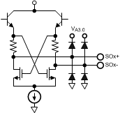 |
Differential High Speed Serial Data Lane pins.
These pins must be AC coupled to the receiving device. The differential trace routing from these pins must maintain a 100 Ω characteristic impedance. |
|||
| POWER SUPPLY | ||||||
| VA3.0 | 1, 2 | Supply Input Pin | 3 V Analog Power Supply pin. | |||
| This pin must be connected to a quiet source and decoupled to AGND with a 0.1 µF capacitor located close to each pin and a second 0.1 µF capacitor on bottom layer. | ||||||
| VA1.8 | 15, 16, 28, 39, 40 | Supply Input Pin | 1.8 V Analog Power Supply pins. | |||
| These pins must be connected to a quiet source and decoupled to AGND with a
0.1 µF capacitor located close to each pin and a second 0.1 µF capacitor on bottom layer. |
||||||
| VA1.2 | 21, 29, 35, 36 | Supply Input Pin | 1.2 V Analog Power Supply pins. | |||
| These pins must be connected to a quiet source and decoupled to AGND with a 0.1 µF capacitor located close to each pin and a second 0.1 µF capacitor on bottom layer. | ||||||
| VACLK1.2 | 8, 9 | Supply Input Pin | 1.2 V Analog Power Supply pins for internal clock path. | |||
| These pins must be connected to a quiet source and decoupled to AGND with a 0.1 µF capacitor located close to each pin and a second 0.1 µF capacitor on bottom layer. | ||||||
| AGND | 3, 6, 10, 13, 14, 22, 27, 30, 37, 38 | Analog Ground | Analog Ground. | |||
| Solid ground reference planes under the device are recommended. | ||||||
| Exposed Thermal Pad | Exposed Thermal Pad. | |||||
| The exposed pad must be connected to the AGND ground plane electrically and with good thermal dissipation properties to ensure rated performance. | ||||||