ZHCSE48B September 2015 – January 2019 ADC31JB68
PRODUCTION DATA.
- 1 特性
- 2 应用
- 3 说明
- 4 修订历史记录
- 5 Pin Configuration and Functions
- 6 Specifications
- 7 Parameter Measurement Information
-
8 Detailed Description
- 8.1 Overview
- 8.2 Functional Block Diagram
- 8.3
Feature Description
- 8.3.1 Analog Inputs and Input Buffer
- 8.3.2 Amplitude and Phase Imbalance Correction
- 8.3.3 Over-Range Detection
- 8.3.4 Input Clock Divider
- 8.3.5 SYSREF Detection Gate
- 8.3.6 Serial Differential Output Drivers
- 8.3.7 ADC Core Calibration
- 8.3.8 Data Format
- 8.3.9 JESD204B Supported Features
- 8.3.10 JESD204B Interface
- 8.3.11 Transport Layer Configuration
- 8.3.12 Test Pattern Sequences
- 8.3.13 JESD204B Link Initialization
- 8.3.14 SPI
- 8.4 Device Functional Modes
- 8.5
Register Map
- 8.5.1
Register Descriptions
- 8.5.1.1 CONFIG_A (address = 0x0000) [reset = 0x3C]
- 8.5.1.2 DEVICE CONFIG (address = 0x0002) [reset = 0x00]
- 8.5.1.3 CHIP_TYPE (address = 0x0003 ) [reset = 0x03]
- 8.5.1.4 CHIP_ID (address = 0x0005, 0x0004) [reset = 0x00, 0x1B]
- 8.5.1.5 CHIP_VERSION (address =0x0006) [reset = 0x00]
- 8.5.1.6 VENDOR_ID (address = 0x000D, 0x000C) [reset = 0x04, 0x51]
- 8.5.1.7 SPI_CFG (address = 0x0010 ) [reset = 0x01]
- 8.5.1.8 OM1 (Operational Mode 1) (address = 0x0012) [reset = 0xC1]
- 8.5.1.9 OM2 (Operational Mode 2) (address = 0x0013) [reset = 0x20]
- 8.5.1.10 IMB_ADJ (Imbalance Adjust) (address = 0x0014) [reset = 0x00]
- 8.5.1.11 OVR_EN (Over-Range Enable) (address = 0x003A) [reset = 0x00]
- 8.5.1.12 OVR_HOLD (Over-Range Hold) (address = 0x003B) [reset = 0x00]
- 8.5.1.13 OVR_TH (Over-Range Threshold) (address = 0x003C) [reset = 0x00]
- 8.5.1.14 DC_MODE (DC Offset Correction Mode) (address = 0x003D) [reset = 0x00]
- 8.5.1.15 SER_CFG (Serial Lane Transmitter Configuration) (address = 0x0047) [reset = 0x00]
- 8.5.1.16 JESD_CTRL1 (JESD Configuration Control 1) (address = 0x0060) [reset = 0x7F]
- 8.5.1.17 JESD_CTRL2 (JESD Configuration Control 2) (address = 0x0061) [reset = 0x00]
- 8.5.1.18 JESD_RSTEP (JESD Ramp Pattern Step) (address = 0x0063, 0x0062) [reset = 0x00, 0x01]
- 8.5.1.19 SER_INV (Serial Lane Inversion Control) (address = 0x0064) [reset = 0x00]
- 8.5.1.20 JESD_STATUS (JESD Link Status) (address = 0x006C) [reset = N/A]
- 8.5.1
Register Descriptions
- 9 Application and Implementation
- 10Power Supply Recommendations
- 11Layout
- 12器件和文档支持
- 13机械、封装和可订购信息
9.1.2.4 Driving the Analog Input
The analog input may be driven by a number of network types depending on the end application. The most important design aspects to consider when designing the ADC voltage driver network are signal coupling, impedance matching, differential signal balance, anti-alias filtering, and signal level.
An analog signal is AC or DC coupled to the ADC depending on whether signal frequencies near DC must be sampled without attenuation. DC coupling requires tight control of the output common-mode of the ADC driver to match the input common-mode of the ADC input. In the case of DC coupling, the bias at the VCM pin may be used as a reference to set the driver output common-mode, but the load cannot source or sink more current than the specified value in the electrical parameters. AC coupling does not require strict common-mode control of the driver and is typically achieved using AC coupling capacitors or a flux-coupled transformer. AC coupling capacitors should be chosen to have 0.1-Ω impedance or less over the frequency band of interest. LC filter designs may be customized to achieve either AC or DC coupling.
The internal input network of the ADC31JB68 device has the common-mode voltage bias provided through internal shunt termination resistors. The recommended bias for the external termination resistors is the common-mode reference voltage from the VCM pin.
Impedance matching in high speed signal paths using an ADC is dictated by the characteristic impedance of interconnects and by the design of anti-aliasing filters. Matching the source to the load termination is critical to ensure maximum power transfer to the load and to maintain gain flatness across the desired frequency band. In applications with signal transmission lengths greater than 10% of the smallest signal wavelength (0.1 λ), matching is also desirable to avoid signal reflections and other transmission line effects. Applications that require high order anti-aliasing filters designs, including LC bandpass filters, require an expected source and load termination to ensure the passband bandwidth and ripple of the filter design. The recommended range of the ADC total load termination is from 50- to 200-Ω differential. The ADC31JB68 device has an internal differential load termination, but additional termination resistance may be added at the ADC input pins to adjust the total termination. The load termination at the ADC input presents a system-level design tradeoff. Better 2nd order distortion performance (HD2, IMD2) is achieved by the ADC using a lower load termination resistance, but the ADC driver must have a higher drive strength and linearity to drive the lower impedance. Choosing a 100-Ω total load termination is a reasonable balance between these opposing requirements.
Differential signal balance is important to achieve high distortion performance, particularly even order distortion (HD2, HD4). Circuits such as transformers and filters in the signal path between the signal source and ADC can disrupt the amplitude and phase balance of the differential signal before reaching the ADC input due to component tolerances or parasitic mismatches between the two parallel paths of the differential signal. Driving the ADC31JB68 device with a single-ended signal is not supported due to the tight restriction on the ADC input common-mode to maintain good distortion performance.
Converting a single-ended signal to a differential signal may be performed by an ADC driver or transformer. The advantages of the ADC driver over a transformer include configurable gain, isolation from previous stages of analog signal processing, and superior differential signal balancing. The advantages of using a transformer include no additional power consumption and little additional noise or distortion.
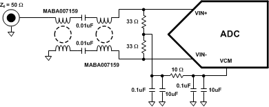
 Figure 67. Transformer Input Network
 Figure 67 is an example of driving the ADC input with a cascaded transformer configuration. The cascaded transformer configuration provides a high degree of differential signal balancing, the series 0.01-µF capacitors provide AC coupling, and the additional 33-Ω termination resistors provide a total differential load termination of 50 Ω. When additional termination resistors are added to change the ADC load termination, shunt terminations to the VCM reference are recommended to reduce common-mode fluctuations or sources of common-mode interference. A differential termination may be used if these sources of common-mode interference are minimal. In either case, the additional termination components must be placed as close to the ADC pins as possible. The MABA007159 transmission-line transformer from this example is widely available and results in good differential balance. Shunt capacitors at the ADC input, used to suppress the charge kickback of an ADC with switched-capacitor inputs, are not required for this purpose because the buffered input of the ADC31JB68 device does not kick back a significant amount of charge.
The insertion loss between an ADC driver and the ADC input is important because the driver must overcome the insertion loss of the connecting network to drive the ADC to full-scale and achieve the best SNR. Minimizing the loss through the network reduces the output swing and distortion requirements of the driver and usually translates to a system-level power savings in the driver. This can be accomplished by selecting transformers or filter designs with low insertion loss. Some filter designs may employ reduced source terminations or impedance conversions to minimize loss. Many designs require the use of high-Q inductors and capacitors to achieve an expected passband flatness and profile.
Sampling theory states that if a signal with frequency ƒIN is sampled at a rate less than 2 × ƒIN, then it experiences aliasing, causing the signal to fall at a new frequency between 0 and FS / 2 in the sampled spectrum and become indistinguishable from other signals at that new frequency.
To prevent out-of-band interference from aliasing onto a desired signal at a particular frequency, an anti-aliasing filter is required at the ADC input to attenuate the interference to a level below the level of the desired signal. This is accomplished by a lowpass filter in systems with desired signals from DC to FS / 2 or with a bandpass filter in systems with desired signals greater than FS / 2 (under-sampled signals). If an appropriate anti-aliasing filter is not included in the system design, the system may suffer from reduced dynamic range due to additional noise and distortion that aliases into the frequency bandwidth of interest.
An anti-aliasing filter is required in front of the ADC input in most applications to attenuate noise and distortion at frequencies that alias into any important frequency band of interest during the sampling process. An anti-aliasing filter is typically a LC lowpass or bandpass filter with low insertion loss. The bandwidth of the filter is typically designed to be less than FS / 2 to allow room for the filter transition bands. Figure 68 is an example architecture of a 9 pole order LC bandpass anti-aliasing filter with added transmission zeros that can achieve a tight filtering profile for second Nyquist zone under-sampling applications.
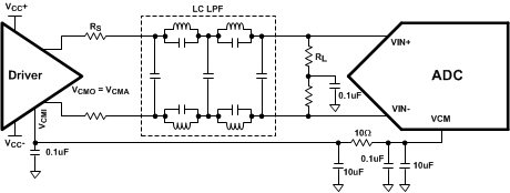
 Figure 69. DC Coupled Interface
 DC coupling to the analog input is also possible but the input common-mode must be tightly controlled for specified performance. The driver device must have an output common-mode that matches the input common-mode of the ADC31JB68 device and the driver must track the VCM output from the ADC31JB68 device, as shown in the example DC coupled interface of Figure 69, because the input common-mode varies with temperature. The common-mode path from the VCM output, through the driver device, back to the ADC31JB68 device input, and through a common-mode detector inside the ADC31JB68 device forms a closed tracking loop that will correct common-mode offset contributed by the driver device but the loop must be stable to ensure correct performance. The loop requires the large, 10-µF capacitor at the VCM output to establish the dominant pole for stability and the driver device must reliably track the VCM output voltage bias.
