ZHCSE48B September 2015 – January 2019 ADC31JB68
PRODUCTION DATA.
- 1 特性
- 2 应用
- 3 说明
- 4 修订历史记录
- 5 Pin Configuration and Functions
- 6 Specifications
- 7 Parameter Measurement Information
-
8 Detailed Description
- 8.1 Overview
- 8.2 Functional Block Diagram
- 8.3
Feature Description
- 8.3.1 Analog Inputs and Input Buffer
- 8.3.2 Amplitude and Phase Imbalance Correction
- 8.3.3 Over-Range Detection
- 8.3.4 Input Clock Divider
- 8.3.5 SYSREF Detection Gate
- 8.3.6 Serial Differential Output Drivers
- 8.3.7 ADC Core Calibration
- 8.3.8 Data Format
- 8.3.9 JESD204B Supported Features
- 8.3.10 JESD204B Interface
- 8.3.11 Transport Layer Configuration
- 8.3.12 Test Pattern Sequences
- 8.3.13 JESD204B Link Initialization
- 8.3.14 SPI
- 8.4 Device Functional Modes
- 8.5
Register Map
- 8.5.1
Register Descriptions
- 8.5.1.1 CONFIG_A (address = 0x0000) [reset = 0x3C]
- 8.5.1.2 DEVICE CONFIG (address = 0x0002) [reset = 0x00]
- 8.5.1.3 CHIP_TYPE (address = 0x0003 ) [reset = 0x03]
- 8.5.1.4 CHIP_ID (address = 0x0005, 0x0004) [reset = 0x00, 0x1B]
- 8.5.1.5 CHIP_VERSION (address =0x0006) [reset = 0x00]
- 8.5.1.6 VENDOR_ID (address = 0x000D, 0x000C) [reset = 0x04, 0x51]
- 8.5.1.7 SPI_CFG (address = 0x0010 ) [reset = 0x01]
- 8.5.1.8 OM1 (Operational Mode 1) (address = 0x0012) [reset = 0xC1]
- 8.5.1.9 OM2 (Operational Mode 2) (address = 0x0013) [reset = 0x20]
- 8.5.1.10 IMB_ADJ (Imbalance Adjust) (address = 0x0014) [reset = 0x00]
- 8.5.1.11 OVR_EN (Over-Range Enable) (address = 0x003A) [reset = 0x00]
- 8.5.1.12 OVR_HOLD (Over-Range Hold) (address = 0x003B) [reset = 0x00]
- 8.5.1.13 OVR_TH (Over-Range Threshold) (address = 0x003C) [reset = 0x00]
- 8.5.1.14 DC_MODE (DC Offset Correction Mode) (address = 0x003D) [reset = 0x00]
- 8.5.1.15 SER_CFG (Serial Lane Transmitter Configuration) (address = 0x0047) [reset = 0x00]
- 8.5.1.16 JESD_CTRL1 (JESD Configuration Control 1) (address = 0x0060) [reset = 0x7F]
- 8.5.1.17 JESD_CTRL2 (JESD Configuration Control 2) (address = 0x0061) [reset = 0x00]
- 8.5.1.18 JESD_RSTEP (JESD Ramp Pattern Step) (address = 0x0063, 0x0062) [reset = 0x00, 0x01]
- 8.5.1.19 SER_INV (Serial Lane Inversion Control) (address = 0x0064) [reset = 0x00]
- 8.5.1.20 JESD_STATUS (JESD Link Status) (address = 0x006C) [reset = N/A]
- 8.5.1
Register Descriptions
- 9 Application and Implementation
- 10Power Supply Recommendations
- 11Layout
- 12器件和文档支持
- 13机械、封装和可订购信息
9.1.3.1 Driving the CLKIN+ and CLKIN– Input
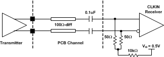
The CLKIN input circuit is composed of a differential receiver and an internal 100-Ω termination to a weakly driven common-mode of 0.5 V. TI recommends AC coupling to the CLKIN input with 0.1-uF external capacitors to maintain the optimal common-mode biasing. Figure 70 shows the CLKIN receiver circuit and an example AC coupled interface.
 Figure 70. Driving the CLKIN Input With an AC Coupled Interface
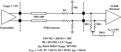
 DC coupling is allowed as long as the input common-mode range requirements are satisfied. The input common-mode of the CLKIN input is not compatible with many common signaling standards like LVDS and LVPECL. Therefore, the CLKIN signal driver common-mode must be customized at the transmitter or adjusted along the interface. Figure 71 shows an example DC coupled interface that uses a resistor divider network to reduce the common-mode while maintaining a 100-Ω total termination at the load. Design equations are provided with example values to determine the resistor values.
 Figure 71. Driving the CLKIN Input With an Example DC Coupled Interface
 The CLKIN input supports any type of standard signaling that meets the input signal swing and common-mode range requirements with an appropriate interface. Generic differential sinusoidal or square-wave clock signals are also supported. TI does not recommend driving the CLKIN input single-ended. The differential lane trace on the PCB should be designed to be a controlled 100 Ω and protected from noise sources or other interfering signals.