SBAS860 August 2017 ADC31RF80
PRODUCTION DATA.
- 1 Features
- 2 Applications
- 3 Description
- 4 Revision History
- 5 Pin Configuration and Functions
-
6 Specifications
- 6.1 Absolute Maximum Ratings
- 6.2 ESD Ratings
- 6.3 Recommended Operating Conditions
- 6.4 Thermal Information
- 6.5 Electrical Characteristics
- 6.6 AC Performance Characteristics: fS = 2949.12 MSPS
- 6.7 AC Performance Characteristics: fS = 2457.6 MSPS (Performance Optimized for F + A + D Band)
- 6.8 AC Performance Characteristics: fS = 2457.6 MSPS (Performance Optimized for F + A Band)
- 6.9 Digital Requirements
- 6.10 Timing Requirements
- 6.11 Typical Characteristics
- 7 Parameter Measurement Information
-
8 Detailed Description
- 8.1 Overview
- 8.2 Functional Block Diagram
- 8.3
Feature Description
- 8.3.1 Analog Inputs
- 8.3.2 Clock Input
- 8.3.3 SYSREF Input
- 8.3.4 DDC Block
- 8.3.5 NCO Switching
- 8.3.6 SerDes Transmitter Interface
- 8.3.7 Eye Diagrams
- 8.3.8 Alarm Outputs: Power Detectors for AGC Support
- 8.3.9 Power-Down Mode
- 8.3.10 ADC Test Pattern
- 8.4
Device Functional Modes
- 8.4.1 Device Configuration
- 8.4.2
JESD204B Interface
- 8.4.2.1 JESD204B Initial Lane Alignment (ILA)
- 8.4.2.2 JESD204B Frame Assembly
- 8.4.2.3 JESD204B Frame Assembly with Decimation (Single-Band DDC): Complex Output
- 8.4.2.4 JESD204B Frame Assembly with Decimation (Single-Band DDC): Real Output
- 8.4.2.5 JESD204B Frame Assembly with Decimation (Single-Band DDC): Real Output
- 8.4.2.6 JESD204B Frame Assembly with Decimation (Dual-Band DDC): Complex Output
- 8.4.2.7 JESD204B Frame Assembly with Decimation (Dual-Band DDC): Real Output
- 8.4.3 Serial Interface
- 8.5
Register Maps
- 8.5.1 Example Register Writes
- 8.5.2
Register Descriptions
- 8.5.2.1
General Registers
- 8.5.2.1.1 Register 000h (address = 000h), General Registers
- 8.5.2.1.2 Register 002h (address = 002h), General Registers
- 8.5.2.1.3 Register 003h (address = 003h), General Registers
- 8.5.2.1.4 Register 004h (address = 004h), General Registers
- 8.5.2.1.5 Register 010h (address = 010h), General Registers
- 8.5.2.1.6 Register 011h (address = 011h), General Registers
- 8.5.2.1.7 Register 012h (address = 012h), General Registers
- 8.5.2.1
General Registers
- 8.5.3
Master Page (M = 0)
- 8.5.3.1 Register 020h (address = 020h), Master Page
- 8.5.3.2 Register 032h (address = 032h), Master Page
- 8.5.3.3 Register 039h (address = 039h), Master Page
- 8.5.3.4 Register 03Ch (address = 03Ch), Master Page
- 8.5.3.5 Register 05Ah (address = 05Ah), Master Page
- 8.5.3.6 Register 03Dh (address = 3Dh), Master Page
- 8.5.3.7 Register 057h (address = 057h), Master Page
- 8.5.3.8 Register 058h (address = 058h), Master Page
- 8.5.4 ADC Page (FFh, M = 0)
- 8.5.5 Digital Function Page (610000h, M = 1)
- 8.5.6 Offset Corr Page (610000h, M = 1)
- 8.5.7 Digital Gain Page (610005h, M = 1)
- 8.5.8
Main Digital Page (680000h, M = 1)
- 8.5.8.1 Register 000h (address = 000h), Main Digital Page
- 8.5.8.2 Register 0A2h (address = 0A2h), Main Digital Page
- 8.5.8.3 Register 0A5h (address = 0A5h), Main Digital Page
- 8.5.8.4 Register 0A9h (address = 0A9h), Main Digital Page
- 8.5.8.5 Register 0B0h (address = 0B0h), Main Digital Page
- 8.5.8.6 Register 0B1h (address = 0B1h), Main Digital Page
- 8.5.8.7 Register 0B2h (address = 0B2h), Main Digital Page
- 8.5.8.8 Register 0B3h (address = 0B3h), Main Digital Page
- 8.5.8.9 Register 0B4h (address = 0B4h), Main Digital Page
- 8.5.8.10 Register 0B5h (address = 0B5h), Main Digital Page
- 8.5.8.11 Register 0B6h (address = 0B6h), Main Digital Page
- 8.5.8.12 Register 0B7h (address = 0B7h), Main Digital Page
- 8.5.8.13 Register 0B8h (address = 0B8h), Main Digital Page
- 8.5.8.14 Register 0B9h (address = 0B9h), Main Digital Page
- 8.5.8.15 Register 0BAh (address = 0BAh), Main Digital Page
- 8.5.8.16 Register 0BBh (address = 0BBh), Main Digital Page
- 8.5.9
JESD Digital Page (6900h, M = 1)
- 8.5.9.1 Register 001h (address = 001h), JESD Digital Page
- 8.5.9.2 Register 002h (address = 002h ), JESD Digital Page
- 8.5.9.3 Register 003h (address = 003h), JESD Digital Page
- 8.5.9.4 Register 004h (address = 004h), JESD Digital Page
- 8.5.9.5 Register 006h (address = 006h), JESD Digital Page
- 8.5.9.6 Register 007h (address = 007h), JESD Digital Page
- 8.5.9.7 Register 016h (address = 016h), JESD Digital Page
- 8.5.9.8 Register 017h (address = 017h), JESD Digital Page
- 8.5.9.9 Register 032h-035h (address = 032h-035h), JESD Digital Page
- 8.5.9.10 Register 036h (address = 036h), JESD Digital Page
- 8.5.9.11 Register 037h (address = 037h), JESD Digital Page
- 8.5.9.12 Register 03Ch (address = 03Ch), JESD Digital Page
- 8.5.9.13 Register 03Eh (address = 03Eh), JESD Digital Page
- 8.5.10
Decimation Filter Page
- 8.5.10.1 Register 000h (address = 000h), Decimation Filter Page
- 8.5.10.2 Register 001h (address = 001h), Decimation Filter Page
- 8.5.10.3 Register 002h (address = 2h), Decimation Filter Page
- 8.5.10.4 Register 005h (address = 005h), Decimation Filter Page
- 8.5.10.5 Register 007h (address = 007h), Decimation Filter Page
- 8.5.10.6 Register 008h (address = 008h), Decimation Filter Page
- 8.5.10.7 Register 009h (address = 009h), Decimation Filter Page
- 8.5.10.8 Register 00Ah (address = 00Ah), Decimation Filter Page
- 8.5.10.9 Register 00Bh (address = 00Bh), Decimation Filter Page
- 8.5.10.10 Register 00Ch (address = 00Ch), Decimation Filter Page
- 8.5.10.11 Register 00Dh (address = 00Dh), Decimation Filter Page
- 8.5.10.12 Register 00Eh (address = 00Eh), Decimation Filter Page
- 8.5.10.13 Register 00Fh (address = 00Fh), Decimation Filter Page
- 8.5.10.14 Register 010h (address = 010h), Decimation Filter Page
- 8.5.10.15 Register 011h (address = 011h), Decimation Filter Page
- 8.5.10.16 Register 014h (address = 014h), Decimation Filter Page
- 8.5.10.17 Register 016h (address = 016h), Decimation Filter Page
- 8.5.10.18 Register 01Eh (address = 01Eh), Decimation Filter Page
- 8.5.10.19 Register 01Fh (address = 01Fh), Decimation Filter Page
- 8.5.10.20 Register 033h-036h (address = 033h-036h), Decimation Filter Page
- 8.5.10.21 Register 037h (address = 037h), Decimation Filter Page
- 8.5.10.22 Register 038h (address = 038h), Decimation Filter Page
- 8.5.10.23 Register 039h (address = 039h), Decimation Filter Page
- 8.5.10.24 Register 03Ah (address = 03Ah), Decimation Filter Page
- 8.5.11
Power Detector Page
- 8.5.11.1 Register 000h (address = 000h), Power Detector Page
- 8.5.11.2 Register 001h-002h (address = 001h-002h), Power Detector Page
- 8.5.11.3 Register 003h (address = 003h), Power Detector Page
- 8.5.11.4 Register 007h-00Ah (address = 007h-00Ah), Power Detector Page
- 8.5.11.5 Register 00Bh-00Ch (address = 00Bh-00Ch), Power Detector Page
- 8.5.11.6 Register 00Dh (address = 00Dh), Power Detector Page
- 8.5.11.7 Register 00Eh (address = 00Eh), Power Detector Page
- 8.5.11.8 Register 00Fh, 010h-012h, and 016h-019h (address = 00Fh, 010h-012h, and 016h-019h), Power Detector Page
- 8.5.11.9 Register 013h-01Ah (address = 013h-01Ah), Power Detector Page
- 8.5.11.10 Register 01Dh-01Eh (address = 01Dh-01Eh), Power Detector Page
- 8.5.11.11 Register 020h (address = 020h), Power Detector Page
- 8.5.11.12 Register 021h (address = 021h), Power Detector Page
- 8.5.11.13 Register 022h-025h (address = 022h-025h), Power Detector Page
- 8.5.11.14 Register 027h (address = 027h), Power Detector Page
- 8.5.11.15 Register 02Bh (address = 02Bh), Power Detector Page
- 8.5.11.16 Register 032h-035h (address = 032h-035h), Power Detector Page
- 8.5.11.17 Register 037h (address = 037h), Power Detector Page
- 8.5.11.18 Register 038h (address = 038h), Power Detector Page
- 9 Application and Implementation
- 10Power Supply Recommendations
- 11Layout
- 12Device and Documentation Support
- 13Mechanical, Packaging, and Orderable Information
6 Specifications
6.1 Absolute Maximum Ratings
over operating free-air temperature range (unless otherwise noted)(1)| MIN | MAX | UNIT | ||
|---|---|---|---|---|
| Supply voltage range | AVDD19 | –0.3 | 2.1 | V |
| AVDD | –0.3 | 1.4 | ||
| DVDD | –0.3 | 1.4 | ||
| Voltage applied to input pins | INP, INM | –0.3 | AVDD19 + 0.3 | V |
| CLKINP, CLKINM | –0.3 | AVDD + 0.6 | ||
| SYSREFP, SYSREFM, SYNCBP, SYNCBM | –0.3 | AVDD + 0.6 | ||
| SCLK, SEN, SDIN, RESET, PDN, GPIO1, GPIO2, GPIO3, GPIO4 | –0.2 | AVDD19 + 0.2 | ||
| Voltage applied to output pins | –0.3 | 2.2 | V | |
| Temperature | Operating free-air, TA | –40 | 85 | °C |
| Storage, Tstg | –65 | 150 | ||
(1) Stresses beyond those listed under Absolute Maximum Ratings may cause permanent damage to the device. These are stress ratings only, which do not imply functional operation of the device at these or any other conditions beyond those indicated under Recommended Operating Conditions. Exposure to absolute-maximum-rated conditions for extended periods may affect device reliability.
6.2 ESD Ratings
| VALUE | UNIT | |||
|---|---|---|---|---|
| V(ESD) | Electrostatic discharge | Human-body model (HBM), per ANSI/ESDA/JEDEC JS-001(1) | ±1000 | V |
| Charged-device model (CDM), per JEDEC specification JESD22-C101(2) | ±500 | |||
(1) JEDEC document JEP155 states that 500-V HBM allows safe manufacturing with a standard ESD control process.
(2) JEDEC document JEP157 states that 250-V CDM allows safe manufacturing with a standard ESD control process.
6.3 Recommended Operating Conditions
over operating free-air temperature range (unless otherwise noted)| MIN | NOM | MAX | UNIT | ||
|---|---|---|---|---|---|
| Supply voltage(2) | AVDD19 | 1.8 | 1.9 | 2.0 | V |
| AVDD | 1.1 | 1.15 | 1.25 | ||
| DVDD | 1.1 | 1.15 | 1.2 | ||
| Temperature | Operating free-air, TA | –40 | 85 | °C | |
| Operating junction, TJ | 105(1) | 125 | |||
(1) Prolonged use above this junction temperature may increase the device failure-in-time (FIT) rate.
(2) Always power up the DVDD supply (1.15 V) before the AVDD19 (1.9 V) supply. The AVDD (1.15 V) supply can come up in any order.
6.4 Thermal Information
| THERMAL METRIC(1) | ADC31RF80 | UNIT | |
|---|---|---|---|
| RMP (VQFN) | |||
| 72 PINS | |||
| RθJA | Junction-to-ambient thermal resistance | 21.8 | °C/W |
| RθJC(top) | Junction-to-case (top) thermal resistance | 4.4 | °C/W |
| RθJB | Junction-to-board thermal resistance | 2.0 | °C/W |
| ψJT | Junction-to-top characterization parameter | 0.1 | °C/W |
| ψJB | Junction-to-board characterization parameter | 2.0 | °C/W |
| RθJC(bot) | Junction-to-case (bottom) thermal resistance | 0.2 | °C/W |
(1) For more information about traditional and new thermal metrics, see the Semiconductor and IC Package Thermal Metrics application report.
6.5 Electrical Characteristics
typical values are specified at an ambient temperature of 25°C; minimum and maximum values are specified over an ambient temperature range of –40°C to +85°C; and chip sampling rate = 2949.12 MSPS, 50% clock duty cycle, DDC-bypassed performance, AVDD19 = 1.9 V, AVDD = 1.15 V, DVDD = 1.15 V, –2-dBFS differential input, and 0-dB digital gain (unless otherwise noted)| PARAMETER | TEST CONDITIONS | MIN | TYP | MAX | UNIT | |
|---|---|---|---|---|---|---|
| POWER CONSUMPTION (Divide-by-4, Complex Output Mode(2)) | ||||||
| IAVDD19 | 1.9-V analog supply current | fS = 2949.12 MSPS | 956 | 1439 | mA | |
| IAVDD | 1.15-V analog supply current | fS = 2949.12 MSPS | 499 | 813 | mA | |
| IDVDD | 1.15-V digital supply current | fS = 2949.12 MSPS | 975 | 1164 | mA | |
| PD | Power dissipation | fS = 2949.12 MSPS | 3.51 | 4.71 | W | |
| Global power-down power dissipation | 245 | mW | ||||
| ANALOG INPUTS | ||||||
| Resolution | 14 | Bits | ||||
| Differential input full-scale | 1.35 | VPP | ||||
| VIC | Input common-mode voltage | 1.2(3) | V | |||
| RIN | Input resistance | Differential resistance at dc | 65 | Ω | ||
| CIN | Input capacitance | Differential capacitance at dc | 2 | pF | ||
| VCM common-mode voltage output | 1.2 | V | ||||
| Analog input bandwidth (–3-dB point) |
ADC driven with 50-Ω source | 3200 | MHz | |||
| CLOCK INPUT(1) | ||||||
| Input clock frequency | 1.5 | 3 | GSPS | |||
| Differential (peak-to-peak) input clock amplitude | 0.5 | 1.5 | 2.5 | VPP | ||
| Input clock duty cycle | 45% | 50% | 55% | |||
| Internal clock biasing | 1.0 | V | ||||
| Internal clock termination (differential) | 100 | Ω | ||||
(1) See Figure 79.
(2) Full-scale signal is applied to the analog input; see the Power Consumption in Different Modes section for more details.
(3) When used in dc-coupling mode, the common-mode voltage at the analog inputs should be kept within VCM ±25 mV for best performance.
6.6 AC Performance Characteristics: fS = 2949.12 MSPS
typical values specified at an ambient temperature of 25°C; minimum and maximum values are specified over an ambient temperature range of –40°C to +85°C; and chip sampling rate = 2949.12 MSPS, 50% clock duty cycle, DDC-bypassed performance(5), AVDD19 = 1.9 V, AVDD = 1.15 V, DVDD = 1.15 V, –2-dBFS differential input, and 0-dB digital gain (unless otherwise noted)| PARAMETER | TEST CONDITIONS | MIN(3) | NOM | MAX | UNIT | ||
|---|---|---|---|---|---|---|---|
| SNR | Signal-to-noise ratio | fIN = 100 MHz, AOUT = –2 dBFS | 63.2 | dBFS | |||
| fIN = 900 MHz, AOUT = –2 dBFS | 61.4 | ||||||
| fIN = 1850 MHz, AOUT = –2 dBFS | 56 | 58.5 | |||||
| fIN = 2100 MHz, AOUT = –2 dBFS | 57.7 | ||||||
| fIN = 2600 MHz, AOUT = –2 dBFS | 56.6 | ||||||
| fIN = 3500 MHz, AOUT(2) = –3 dBFS with 2-dB gain | 54.6 | ||||||
| NSD | Noise spectral density averaged across the Nyquist zone | fIN = 100 MHz, AOUT = –2 dBFS | 154.9 | dBFS/Hz | |||
| fIN = 900 MHz, AOUT = –2 dBFS | 153.1 | ||||||
| fIN = 1850 MHz, AOUT = –2 dBFS | 147.7 | 150.2 | |||||
| fIN = 2100 MHz, AOUT = –2 dBFS | 149.4 | ||||||
| fIN = 2600 MHz, AOUT = –2 dBFS | 148.3 | ||||||
| fIN = 3500 MHz, AOUT(2) = –3 dBFS with 2-dB gain | 146.3 | ||||||
| Small-signal SNR | fIN = 1850 MHz, AOUT = –40 dBFS | 63.1 | dBFS | ||||
| NF(1) | Noise figure | fIN = 1850 MHz, AOUT = –40 dBFS | 24.7 | dB | |||
| SINAD | Signal-to-noise and distortion ratio | fIN = 100 MHz, AOUT = –2 dBFS | 62.1 | dBFS | |||
| fIN = 900 MHz, AOUT = –2 dBFS | 61.0 | ||||||
| fIN = 1850 MHz, AOUT = –2 dBFS | 57.8 | ||||||
| fIN = 2100 MHz, AOUT = –2 dBFS | 56.9 | ||||||
| fIN = 2600 MHz, AOUT = –2 dBFS | 55.7 | ||||||
| fIN = 3500 MHz, AOUT(2) = –3 dBFS with 2-dB gain | 54.5 | ||||||
| ENOB | Effective number of bits | fIN = 100 MHz, AOUT = –2 dBFS | 10.0 | Bits | |||
| fIN = 900 MHz, AOUT = –2 dBFS | 9.8 | ||||||
| fIN = 1850 MHz, AOUT = –2 dBFS | 9.3 | ||||||
| fIN = 2100 MHz, AOUT = –2 dBFS | 9.2 | ||||||
| fIN = 2600 MHz, AOUT = –2 dBFS | 9.0 | ||||||
| fIN = 3500 MHz, AOUT(2) = –3 dBFS with 2-dB gain | 8.8 | ||||||
| SFDR | Spurious-free dynamic range | fIN = 100 MHz, AOUT = –2 dBFS | 68.0 | dBc | |||
| fIN = 900 MHz, AOUT = –2 dBFS | 71 | ||||||
| fIN = 1850 MHz, AOUT = –2 dBFS | 58 | 65 | |||||
| fIN = 2100 MHz, AOUT = –2 dBFS | 65 | ||||||
| fIN = 2600 MHz, AOUT = –2 dBFS | 63 | ||||||
| fIN = 3500 MHz, AOUT(2) = –3 dBFS with 2-dB gain | 68 | ||||||
| HD2(4) | Second-order harmonic distortion | fIN = 100 MHz, AOUT = –2 dBFS | 68 | dBc | |||
| fIN = 900 MHz, AOUT = –2 dBFS | 71 | ||||||
| fIN = 1850 MHz, AOUT = –2 dBFS | 58 | 65 | |||||
| fIN = 2100 MHz, AOUT = –2 dBFS | 65 | ||||||
| fIN = 2700 MHz, AOUT = –2 dBFS | 63 | ||||||
| fIN = 3500 MHz, AOUT(2) = –3 dBFS with 2-dB gain | 68 | ||||||
| HD3 | Third-order harmonic distortion | fIN = 100 MHz, AOUT = –2 dBFS | 73 | dBc | |||
| fIN = 900 MHz, AOUT = –2 dBFS | 80 | ||||||
| fIN = 1850 MHz, AOUT = –2 dBFS | 62 | 71 | |||||
| fIN = 2100 MHz, AOUT = –2 dBFS | 77 | ||||||
| fIN = 2600 MHz, AOUT = –2 dBFS | 79 | ||||||
| fIN = 3500 MHz, AOUT(2) = –3 dBFS with 2-dB gain | 76 | ||||||
| HD4, HD5 | Fourth- and fifth-order harmonic distortion | fIN = 100 MHz, AOUT = –2 dBFS | 78 | dBc | |||
| fIN = 900 MHz, AOUT = –2 dBFS | 81.0 | ||||||
| fIN = 1850 MHz, AOUT = –2 dBFS | 69 | 76 | |||||
| fIN = 2100 MHz, AOUT = –2 dBFS | 77 | ||||||
| fIN = 2600 MHz, AOUT = –2 dBFS | 77 | ||||||
| fIN = 3500 MHz, AOUT(2) = –3 dBFS with 2-dB gain | 84 | ||||||
| IL spur | Interleaving spurs: fS / 2 – fIN, fS / 4 ± fIN |
fIN = 100 MHz, AOUT = –2 dBFS | 89 | dBc | |||
| fIN = 900 MHz, AOUT = –2 dBFS | 88 | ||||||
| fIN = 1850 MHz, AOUT = –2 dBFS | 68 | 82 | |||||
| fIN = 2100 MHz, AOUT = –2 dBFS | 79 | ||||||
| fIN = 2600 MHz, AOUT = –2 dBFS | 81 | ||||||
| fIN = 3500 MHz, AOUT(2) = –3 dBFS with 2-dB gain | 75 | ||||||
| HD2 IL | Interleaving spur for HD2: fS / 2 – HD2 |
fIN = 100 MHz, AOUT = –2 dBFS | 85.0 | dBc | |||
| fIN = 900 MHz, AOUT = –2 dBFS | 79.0 | ||||||
| fIN = 1850 MHz, AOUT = –2 dBFS | 62 | 80.0 | |||||
| fIN = 2100 MHz, AOUT = –2 dBFS | 74.0 | ||||||
| fIN = 2600 MHz, AOUT = –2 dBFS | 74.0 | ||||||
| fIN = 3500 MHz, AOUT(2) = –3 dBFS with 2-dB gain | 80.0 | ||||||
| Worst spur | Spurious-free dynamic range (excluding HD2, HD3, HD4, HD5, and interleaving spurs IL and HD2 IL) | fIN = 100 MHz, AOUT = –2 dBFS | 83.0 | dBc | |||
| fIN = 900 MHz, AOUT = –2 dBFS | 76.0 | ||||||
| fIN = 1850 MHz, AOUT = –2 dBFS | 64 | 75.0 | |||||
| fIN = 2100 MHz, AOUT = –2 dBFS | 75.0 | ||||||
| fIN = 2600 MHz, AOUT = –2 dBFS | 75.0 | ||||||
| fIN = 3500 MHz, AOUT(2) = –3 dBFS with 2-dB gain | 72.0 | ||||||
| IMD3 | Two-tone, third-order intermodulation distortion | fIN1 = 900 MHz, fIN2 = 950 MHz, AOUT = –8 dBFS (each tone) |
79 | dBFS | |||
| fIN1 = 1770 MHz, fIN2 = 1790 MHz, AOUT = –8 dBFS (each tone) |
70 | ||||||
| fIN1 = 1800 MHz, fIN2 = 2600 MHz, AOUT = –8 dBFS (each tone) |
73 | ||||||
| fIN1 = 3490 MHz, fIN2 = 3510 MHz, AOUT = –8 dBFS (each tone) with 2-dB gain |
67 | ||||||
(1) The ADC internal resistance = 65 Ω, the driving source resistance = 50 Ω.
(2) Output amplitude, AOUT, refers to the signal amplitude in the ADC digital output that is same as the analog input amplitude, AIN, except when the digital gain feature is used. If digital gain is G, then AOUT = G + AIN.
(3) Minimum values are specified at AOUT = –3 dBFS.
(4) The minimum value of HD2 is specified by bench characterization.
(5) Performance is shown with DDC bypassed. When DDC is enabled, performance improves by the decimation filtering process.
6.7 AC Performance Characteristics: fS = 2457.6 MSPS
(Performance Optimized for F + A + D Band(1))
typical values specified at an ambient temperature of 25°C; minimum and maximum values are specified over an ambient temperature range of –40°C to +85°C; and chip sampling rate = 2949.12 MSPS, 50% clock duty cycle, DDC-bypassed performance, AVDD19 = 1.9 V, AVDD = 1.15 V, DVDD = 1.15 V, –2-dBFS differential input, and 0-dB digital gain (unless otherwise noted)
| PARAMETER | TEST CONDITIONS | MIN | NOM | MAX | UNIT | ||
|---|---|---|---|---|---|---|---|
| SNR | Signal-to-noise ratio | fIN = 1850 MHz, AOUT = –2 dBFS | 58.5 | dBFS | |||
| fIN = 2600 MHz, AOUT = –2 dBFS | 55.8 | ||||||
| SFDR | Spurious-free dynamic range | fIN = 1850 MHz, AOUT = –2 dBFS | 60.0 | dBc | |||
| fIN = 2600 MHz, AOUT = –2 dBFS | 57.0 | ||||||
| HD2 | Second-order harmonic distortion | fIN = 1850 MHz, AOUT = –2 dBFS | 59.0 | dBc | |||
| fIN = 2600 MHz, AOUT = –2 dBFS | 57.0 | ||||||
| HD3 | Third-order harmonic distortion | fIN = 1850 MHz, AOUT = –2 dBFS | 75.0 | dBc | |||
| fIN = 2600 MHz, AOUT = –2 dBFS | 65.0 | ||||||
| IL spur | Interleaving spurs: fS / 2 – fIN, fS / 4 ± fIN |
fIN = 1850 MHz, AOUT = –2 dBFS | 84.0 | dBc | |||
| fIN = 2600 MHz, AOUT = –2 dBFS | 76.0 | ||||||
| HD2 IL | Interleaving spur for HD2: fS / 2 – HD2 |
fIN = 1850 MHz, AOUT = –2 dBFS | 76.0 | dBc | |||
| fIN = 2600 MHz, AOUT = –2 dBFS | 67.0 | ||||||
| IMD3 | Two-tone, third-order intermodulation distortion | fIN1 = 1800 MHz, fIN2 = 2600 MHz, AOUT = –8 dBFS (each tone) |
67.0 | dBFS | |||
(1) F-band = 1880 MHz to 1920 MHz, A-band = 2010 MHz to 2025 MHz, and D-band = 2570 MHz to 2620 MHz.
6.8 AC Performance Characteristics: fS = 2457.6 MSPS
(Performance Optimized for F + A Band(1))
typical values specified at an ambient temperature of 25°C; minimum and maximum values are specified over an ambient temperature range of –40°C to +85°C; and chip sampling rate = 2949.12 MSPS, 50% clock duty cycle, DDC-bypassed performance, AVDD19 = 1.9 V, AVDD = 1.15 V, DVDD = 1.15 V, –2-dBFS differential input, and 0-dB digital gain (unless otherwise noted)
| PARAMETER | TEST CONDITIONS | MIN | NOM | MAX | UNIT | ||
|---|---|---|---|---|---|---|---|
| SNR | Signal-to-noise ratio | fIN = 1850 MHz, AOUT = –2 dBFS | 58.7 | dBFS | |||
| fIN = 2100 MHz, AOUT = –2 dBFS | 57.9 | ||||||
| SFDR | Spurious-free dynamic range | fIN = 1850 MHz, AOUT = –2 dBFS | 71.0 | dBc | |||
| fIN = 2100 MHz, AOUT = –2 dBFS | 69.0 | ||||||
| HD2 | Second-order harmonic distortion | fIN = 1850 MHz, AOUT = –2 dBFS | 71.0 | dBc | |||
| fIN = 2100 MHz, AOUT = –2 dBFS | 69.0 | ||||||
| HD3 | Third-order harmonic distortion | fIN = 1850 MHz, AOUT = –2 dBFS | 75.0 | dBc | |||
| fIN = 2100 MHz, AOUT = –2 dBFS | 76.0 | ||||||
| IL spur | Interleaving spurs: fS / 2 – fIN, fS / 4 ± fIN |
fIN = 1850 MHz, AOUT = –2 dBFS | 82.0 | dBc | |||
| fIN = 2100 MHz, AOUT = –2 dBFS | 84.0 | ||||||
| HD2 IL | Interleaving spur for HD2: fS / 2 – HD2 |
fIN = 1850 MHz, AOUT = –2 dBFS | 80.0 | dBc | |||
| fIN = 2100 MHz, AOUT = –2 dBFS | 80.0 | ||||||
(1) F-band = 1880 MHz to 1920 MHz, A-band = 2010 MHz to 2025 MHz, and D-band = 2570 MHz to 2620 MHz.
6.9 Digital Requirements
typical values are specified at an ambient temperature of 25°C; minimum and maximum values are specified over an ambient temperature range of –40°C to +85°C; and chip sampling rate = 2949.12 MSPS, DDC bypassed performance, 50% clock duty cycle, AVDD19 = 1.9 V, AVDD = 1.15 V, DVDD = 1.15 V, –2-dBFS differential input, and 0-dB digital gain (unless otherwise noted)| PARAMETER | TEST CONDITIONS | MIN | NOM | MAX | UNIT | |
|---|---|---|---|---|---|---|
| DIGITAL INPUTS (RESET, SCLK, SEN, SDIN, PDN, GPIO1, GPIO2, GPIO3, GPIO4) | ||||||
| VIH | High-level input voltage | 0.8 | V | |||
| VIL | Low-level input voltage | 0.4 | V | |||
| IIH | High-level input current | 50 | µA | |||
| IIL | Low-level input current | –50 | µA | |||
| Ci | Input capacitance | 4 | pF | |||
| DIGITAL OUTPUTS (SDOUT, GPIO1, GPIO2, GPIO3, GPIO4) | ||||||
| VOH | High-level output voltage | AVDD19–0.1 | AVDD19 | V | ||
| VOL | Low-level output voltage | 0.1 | V | |||
| DIGITAL INPUTS (SYSREFP and SYSREFM; SYNCBP and SYNCBM; Requires External Biasing) | ||||||
| VID | Differential input voltage | 350 | 450 | 800 | mVPP | |
| VCM | Input common-mode voltage | 1.05 | 1.2 | 1.325 | V | |
| DIGITAL OUTPUTS (JESD204B Interface: D[3:0], Meets JESD204B LV-0IF-11G-SR Standard) | ||||||
| |VOD| | Output differential voltage | 700 | mVPP | |||
| |VOCM| | Output common-mode voltage | 450 | mV | |||
| Transmitter short-circuit current | Transmitter pins shorted to any voltage between –0.25 V and 1.45 V | –100 | 100 | mA | ||
| zos | Single-ended output impedance | 50 | Ω | |||
| Co | Output capacitance | Output capacitance inside the device, from either output to ground | 2 | pF | ||
6.10 Timing Requirements
typical values are specified at an ambient temperature of 25°C; minimum and maximum values are specified over an ambient temperature range of –40°C to +85°C; and chip sampling rate = 2949.12 MSPS, 50% clock duty cycle, DDC-bypassed performance, AVDD19 = 1.9 V, AVDD = 1.15 V, DVDD = 1.15 V, –2-dBFS differential input, and 0-dB digital gain (unless otherwise noted)| MIN | NOM | MAX | UNIT | |||
|---|---|---|---|---|---|---|
| SAMPLE TIMING | ||||||
| Aperture delay | 250 | 750 | ps | |||
| Aperture delay matching between two devices at the same temperature and supply voltage |
±150 | ps | ||||
| Aperture jitter, clock amplitude = 2 VPP | 90 | fS | ||||
| Latency (1)(3) |
Data latency, ADC sample to digital output | DDC block bypassed | 424 | Input clock cycles | ||
| Fast overrange latency, ADC sample to FOVR indication on GPIO pins | 70 | |||||
| tPD | Propagation delay time: logic gates and output buffer delay (does not change with fS) |
6 | ns | |||
| SYSREF TIMING(2) | ||||||
| tSU_SYSREF | SYSREF setup time: referenced to clock rising edge, 2949.12 MSPS | 140 | 70 | ps | ||
| tH_SYSREF | SYSREF hold time: referenced to clock rising edge, 2949.12 MSPS | 50 | 20 | ps | ||
| Valid transition window sampling period: tSU_SYSREF – tH_SYSREF, 2949.12 MSPS | 143 | ps | ||||
| JESD OUTPUT INTERFACE TIMING | ||||||
| UI | Unit interval: 12.5 Gbps | 80 | 100 | 400 | ps | |
| Serial output data rate | 2.5 | 10.0 | 12.5 | Gbps | ||
| Rise, fall times: 1-pF, single-ended load capacitance to ground | 60 | ps | ||||
| Total jitter: BER of 1E-15 and lane rate = 12.5 Gbps | 25 | %UI | ||||
| Random jitter: BER of 1E-15 and lane rate = 12.5 Gbps | 0.99 | %UI, rms | ||||
| Deterministic jitter: BER of 1E-15 and lane rate = 12.5 Gbps | 9.1 | %UI, pk-pk | ||||
(1) Overall latency = latency + tPD.
(2) Common-mode voltage for the SYSREF input is kept at 1.2 V.
(3) Latency increases when the DDC modes are used; see Table 4.
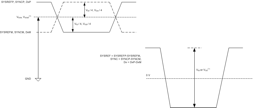
VOCM is not the same as VICM. Similarly, VOD is not the same as VID.
Figure 1. Logic Levels for Digital Inputs and Outputs
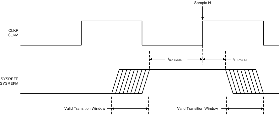 Figure 2. SYSREF Timing Diagram
6.11 Typical Characteristics
typical values are specified at an ambient temperature of 25°C; minimum and maximum values are specified over an ambient temperature range of –40°C to +85°C; and ADC sampling rate = 2949.12 MSPS, DDC bypassed performance, 50% clock duty cycle, AVDD19 = 1.9 V, AVDD = DVDD = 1.15 V, –2-dBFS differential input, and 0-dB digital gain (unless otherwise noted)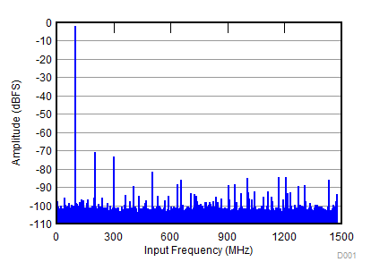
| SNR = 63.4 dBFS; SFDR = 69 dBc; HD2 = –69 dBc; HD3 = –71 dBc; non HD2, HD3 = 80 dBc; IL spur = 82 dBc; fIN = 100 MHz |
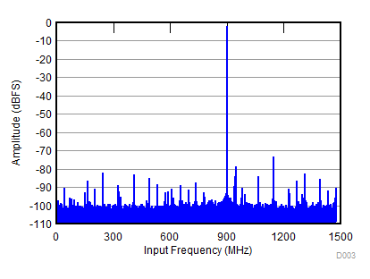
| SNR = 60.8 dBFS; SFDR = 71 dBc; HD2 = –71 dBc; HD3 = –80 dBc; non HD2, HD3 = 83 dBc; IL spur = 83 dBc; fIN = 900 MHz |
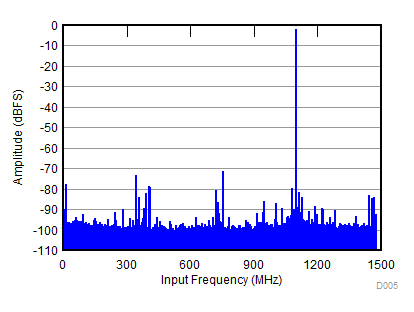
| SNR = 58.9 dBFS; SFDR = 69 dBc; HD2 = –69 dBc; HD3 = –71 dBc; non HD2, HD3 = 77 dBc; IL spur = 76 dBc; fIN = 1.85 GHz |
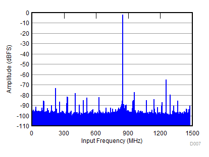
| SNR = 57.9 dBFS; SFDR = 63 dBc; HD2 = –63 dBc; HD3 = –76 dBc; non HD2, HD3 = 78 dBc; IL spur = 73 dBc; fIN = 2.1 GHz |
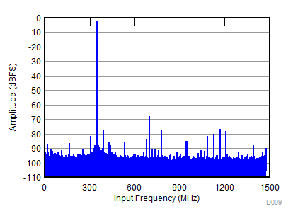
| SNR = 56.8 dBFS; SFDR = 65 dBc; HD2 = –65 dBc; HD3 = –71 dBc; non HD2, HD3 = 89 dBc; IL spur = 74 dBc; fIN = 2.6 GHz |
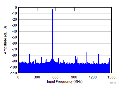
| SNR = 54.6 dBFS; SFDR = 70 dBc; HD2 = –72 dBc; HD3 = –74 dBc; non HD2, HD3 = 70 dBc; IL spur = 76 dBc; fIN = 3.5 GHz, AIN = –3 dBFS with 2-dB gain |
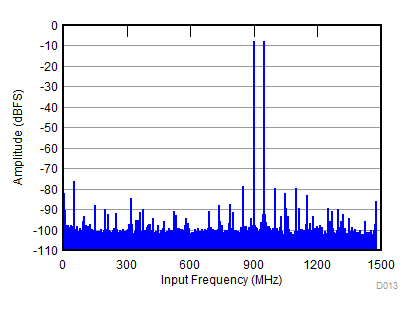
| fIN1 = 900 MHz, fIN2 = 950 MHz, AIN = –8 dBFS, IMD = 79 dBFS |
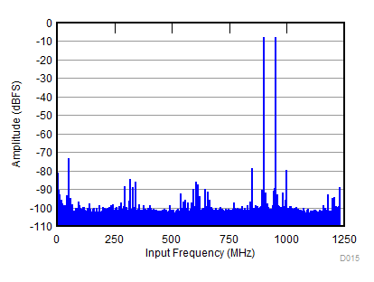
| fIN1 = 900 MHz, fIN2 = 950 MHz, AIN = –8 dBFS, IMD = 78 dBFS | ||
(–8 dBFS, fS = 2457.6 MSPS)
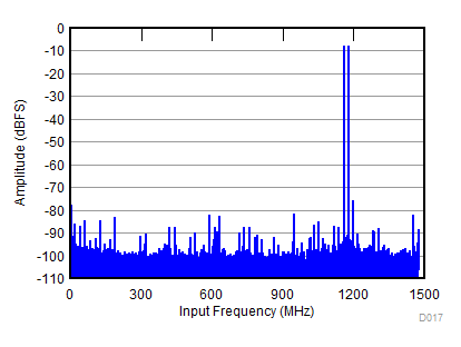
| fIN1 = 1.77 GHz, fIN2 = 1.79 GHz, AIN = –8 dBFS, IMD = 75 dBFS | ||
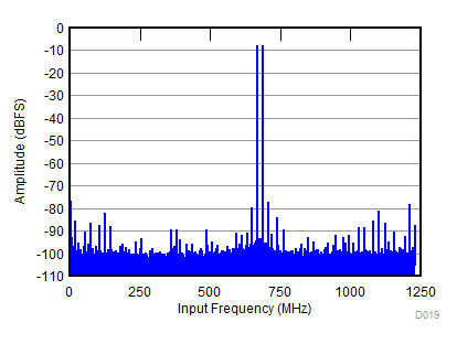
| fIN1 = 1.77 GHz, fIN2 = 1.79 GHz, AIN = –8 dBFS, IMD = 76 dBFS |
(–8 dBFS, fS = 2457.6 MSPS)
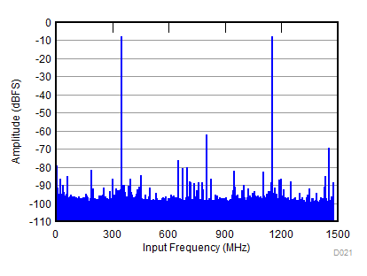
| fIN1 = 1.8 MHz, fIN2 = 2.6 GHz, AIN = –8 dBFS, IMD = 70 dBFS |
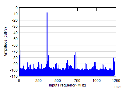
| fIN1 = 2.09 GHz, fIN2 = 2.1 GHz, AIN = –8 dBFS, IMD = 71 dBFS | ||
(–8 dBFS, fS = 2457.6 MSPS)
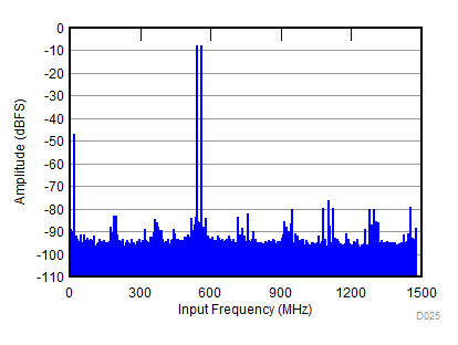
| fIN1 = 3.49 MHz, fIN2 = 3.51 GHz, IMD = 75 dBFS, AIN = –8 dBFS with 2-dB gain |
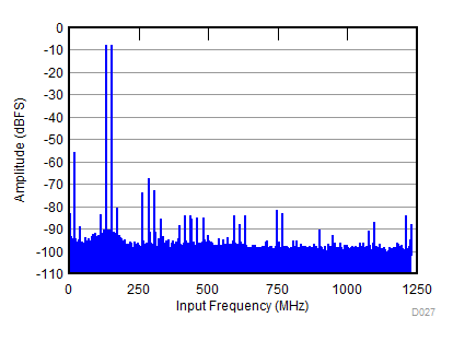
| fIN1 = 2.59 GHz, fIN2 = 2.6 GHz, AIN = –8 dBFS, IMD = 68 dBFS | ||
(–8 dBFS, fS = 2457.6 MSPS)
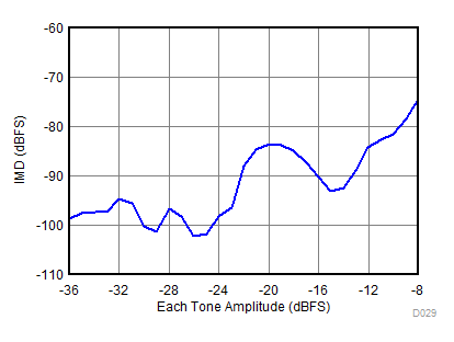
| fIN1 = 1.77 GHz, fIN2 = 1.79 GHz |
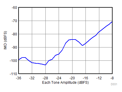
| fIN1 = 1.8 GHz, fIN2 = 2.6 GHz, AIN = –36 dBFS |
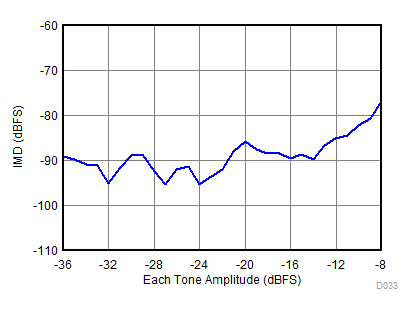
| fIN1 = 3.49 GHz, fIN2 = 3.51 GHz with 2-dB digital gain |
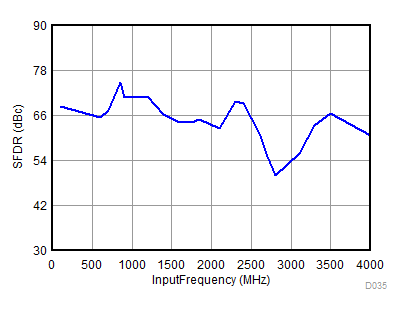
Input Frequency
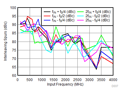
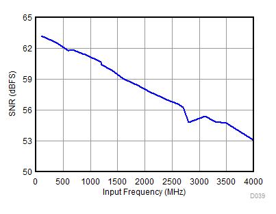
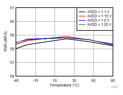
| fIN = 1.85 GHz, AIN = –2 dBFS |
AVDD Supply and Temperature
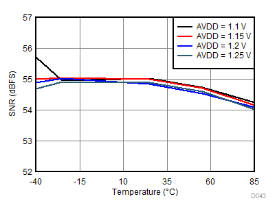
| fIN = 3.5 GHz, AIN = –3 dBFS with 2-dB digital gain |
AVDD Supply and Temperature
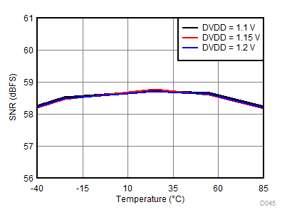
| fIN = 1.85 GHz, AIN = –2 dBFS |
DVDD Supply and Temperature
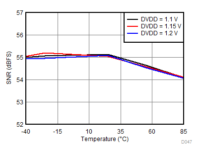
| fIN = 3.5 GHz, AIN = –3 dBFS with 2-dB digital gain |
DVDD Supply and Temperature
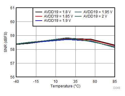
| fIN = 1.85 GHz, AIN = –2 dBFS |
AVDD19 Supply and Temperature
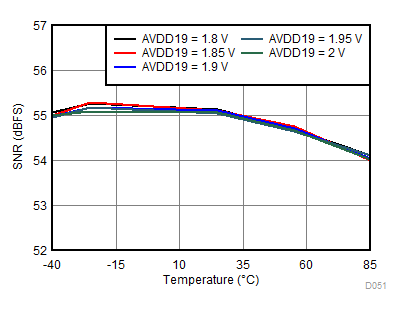
| fIN = 3.5 GHz, AIN = –3 dBFS with 2-dB digital gain |
AVDD19 Supply and Temperature
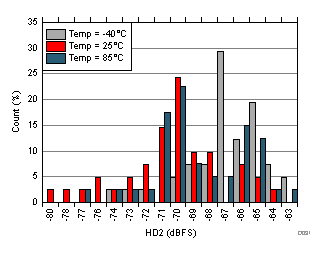
| fIN = 1.78 GHz, AOUT = –2 dBFS |
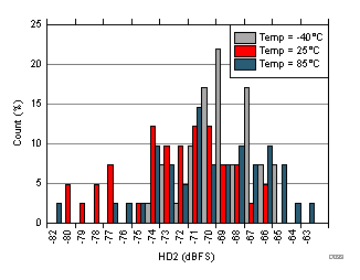
| fIN = 1.78 GHz, AOUT = –2 dBFS |
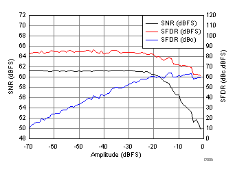
| fIN = 3.5 GHz |
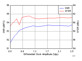
| fIN = 3.5 GHz, AIN = –3 dBFS |
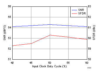
| fIN = 3.5 GHz | ||
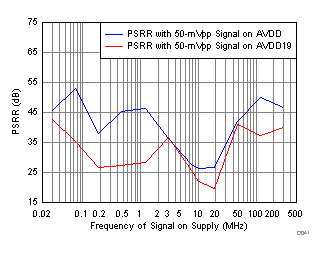
Tone Frequency
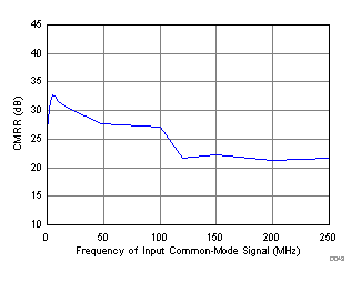
Tone Frequency
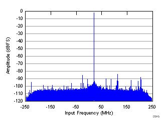
| fIN = 1.78 GHz, AIN = –2 dBFS, fS = 2949.12 MSPS, SNR = 61.6 dBFS, SFDR (includes IL) = 82 dBc |

| fIN = 1.78 GHz, AIN = –2 dBFS, fS = 2949.12 MSPS, SNR = 63 dBFS, SFDR (includes IL) = 82 dBc |
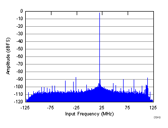
| fIN = 1.78 GHz, AIN = –2 dBFS, fS = 2949.12 MSPS, SNR = 63.7 dBFS, SFDR (includes IL) = 83 dBc |
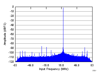
| fIN = 1.78 GHz, AIN = –2 dBFS, fS = 2949.12 MSPS, SNR = 64 dBFS, SFDR (includes IL) = 83 dBc |
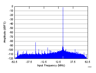
| fIN = 1.78 GHz, AIN = –2 dBFS, fS = 2949.12 MSPS, SNR = 64.4 dBFS, SFDR (includes IL) = 82 dBc |
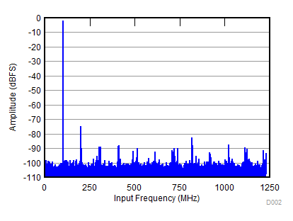
| SNR = 63.3 dBFS; SFDR = 72 dBc; HD2 = –72 dBc; HD3 = –87 dBc; non HD2, HD3 = 85 dBc; IL spur = 80 dBc; fIN = 100 MHz |
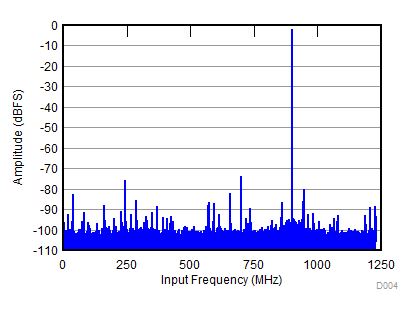
| SNR = 61.4 dBFS; SFDR = 71 dBc; HD2 = –80 dBc; HD3 = –73 dBc; non HD2, HD3 = 74 dBc; IL spur = 80 dBc; fIN = 900 MHz |

| SNR = 58.9 dBFS; SFDR = 71 dBc; HD2 = –71 dBc; HD3 = –75 dBc; non HD2, HD3 = 78 dBc; IL spur = 76 dBc; fIN = 1.85 GHz |
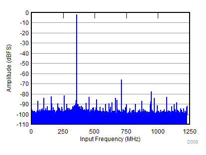
| SNR = 58.2 dBFS; SFDR = 64 dBc; HD2 = –64 dBc; HD3 = –81 dBc; non HD2, HD3 = 83 dBc; IL spur = 80 dBc; fIN = 2.1 GHz |
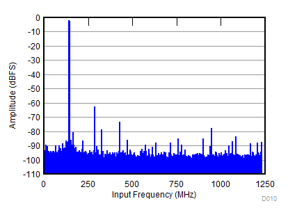
| SNR = 56.8 dBFS; SFDR = 60 dBc; HD2 = –60 dBc; HD3 = –71 dBc; non HD2, HD3 = 73 dBc; IL spur = 75 dBc; fIN = 2.6 GHz |
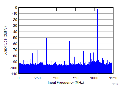
| SNR = 54.9 dBFS; SFDR = 48 dBc; HD2 = –48 dBc; HD3 = –53 dBc; non HD2, HD3 = 68 dBc; IL spur = 69 dBc; fIN = 3.5 GHz, AIN = –3 dBFS with 2-dB gain |
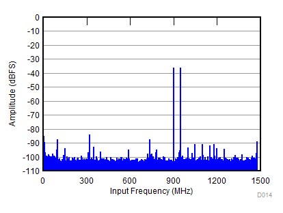
| fIN1 = 900 MHz, fIN2 = 950 MHz, AIN = –36 dBFS, IMD = 94 dBFS |
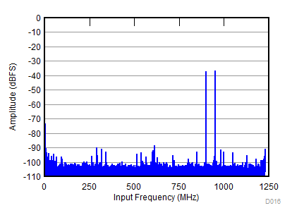
| fIN1 = 900 MHz, fIN2 = 950 MHz, AIN = –36 dBFS, IMD = 92 dBFS |
(–36 dBFS, fS = 2457.6 MSPS)
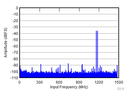
| fIN1 = 1.77 GHz, fIN2 = 1.790 GHz, AIN = –36 dBFS, IMD = 94 dBFS |
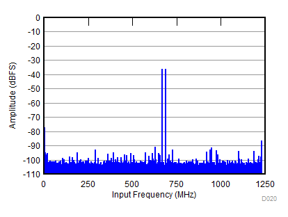
| fIN1 = 1.77 GHz, fIN2 = 1.790 GHz, AIN = –36 dBFS, IMD = 92 dBFS |
(–36 dBFS, fS = 2457.6 MSPS)
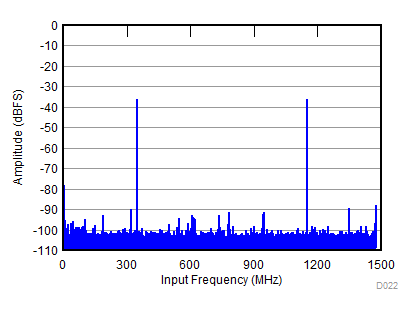
| fIN1 = 1.8 GHz, fIN2 = 2.6 GHz, AIN = –36 dBFS, IMD = 95 dBFS |
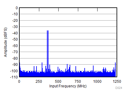
| fIN1 = 2.09 MHz, fIN2 = 2.1 GHz, AIN = –36 dBFS, IMD = 92 dBFS |
(–36 dBFS, fS = 2457.6 MSPS)
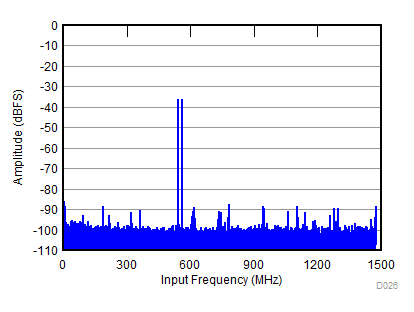
| fIN1 = 3.49 GHz, fIN2 = 3.51 GHz, IMD = 95 dBFS, AIN = –36 dBFS with 2-dB gain |
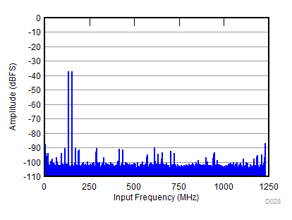
| fIN1 = 2.59 GHz, fIN2 = 2.6 GHz, AIN = –36 dBFS, IMD = 92 dBFS |
(–36 dBFS, fS = 2457.6 MSPS)
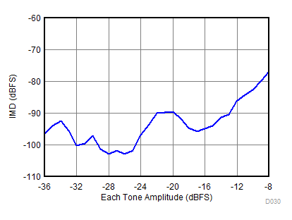
| fIN1 = 1.77 GHz, fIN2 = 1.79 GHz |
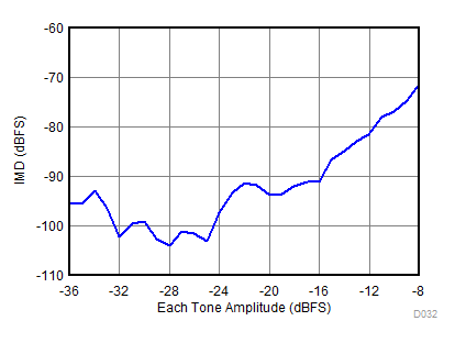
| fIN1 = 2.09 GHz, fIN2 = 2.1 GHz |
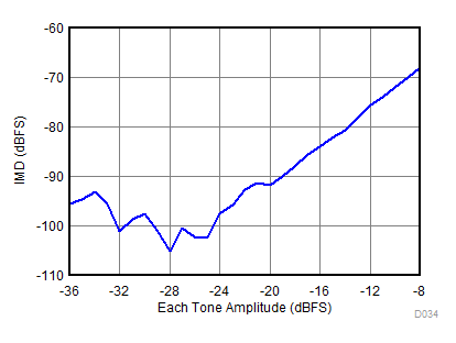
| fIN1 = 2.59GHz, fIN2 = 2.61 GHz |
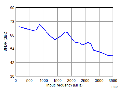
Input Frequency (fS = 2457.6 MSPS)
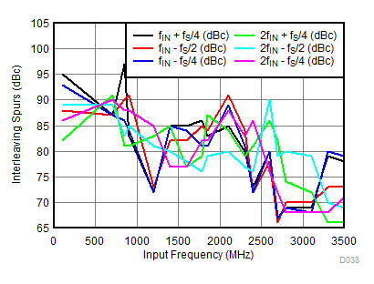
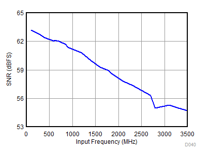
(fS = 2457.6 MSPS)
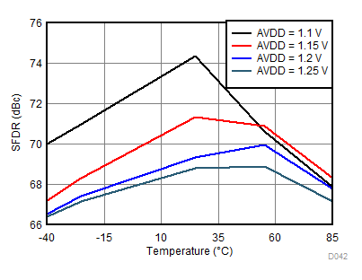
| fIN = 1.85 GHz, AIN = –2 dBFS |
AVDD Supply and Temperature
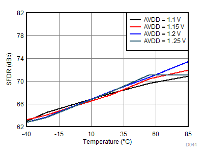
| fIN = 3.5GHz, AIN = –3 dBFS with 2-dB digital gain |
AVDD Supply and Temperature
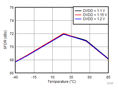
| fIN = 1.85 GHz, AIN = –2 dBFS |
DVDD Supply and Temperature
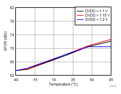
| fIN = 3.5 GHz, AIN = –3 dBFS with 2-dB digital gain |
DVDD Supply and Temperature
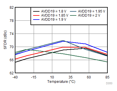
| fIN = 1.85 GHz, AIN = –2 dBFS |
AVDD19 Supply and Temperature
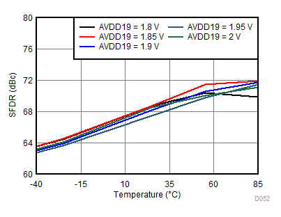
| fIN = 3.5 GHz, AIN = –3 dBFS with 2-dB digital gain |
AVDD19 Supply and Temperature
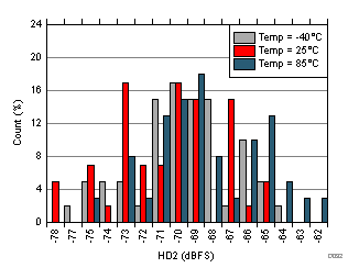
| fIN = 1.78 GHz, AOUT = –2 dBFS |
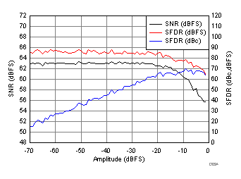
| fIN = 1.78 GHz |
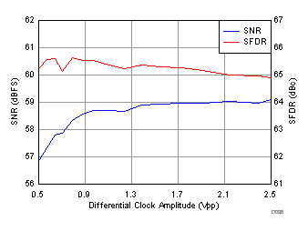
| fIN = 1.78 GHz, AIN = –2 dBFS |
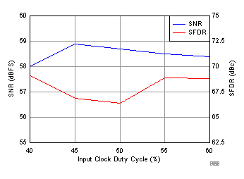
| fIN = 1.78 GHz |
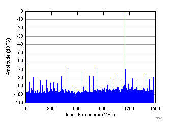
| fIN = 1.8 GHz, AIN = –2 dBFS, PSRR = 37 dB, fPSRR = 3 MHz, APSRR = 50 mVPP, AVDD = 1.9 V |
Test Signal on AVDD Supply
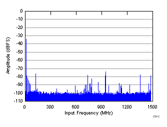
| fCMRR = 10 MHz, APSRR = 50 mVPP, CMRR = 32 dB |
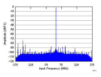
| fIN = 1.78 GHz, AIN = –2 dBFS, fS = 2949.12 MSPS, SNR = 60.6 dBFS, SFDR (includes IL) = 75 dBc |
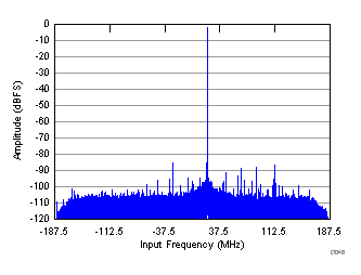
| fIN = 1.78 GHz, AIN = –2 dBFS, fS = 2949.12 MSPS, SNR = 62.6 dBFS, SFDR (includes IL) = 86 dBc |
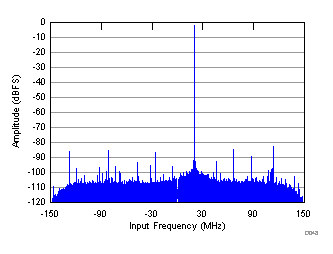
| fIN = 1.78 GHz, AIN = –2 dBFS, fS = 2949.12 MSPS, SNR = 63.3 dBFS, SFDR (includes IL) = 81 dBc |
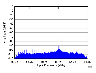
| fIN = 1.78 GHz, AIN = –2 dBFS, fS = 2949.12 MSPS, SNR = 63.9 dBFS, SFDR (includes IL) = 83 dBc |
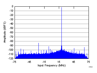
| fIN = 1.78 GHz, AIN = –2 dBFS, fS = 2949.12 MSPS, SNR = 64.4 dBFS, SFDR (includes IL) = 84 dBc |
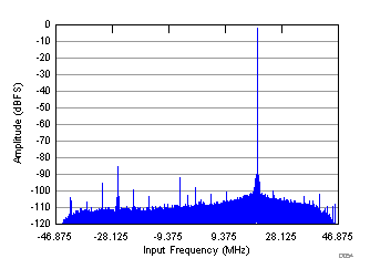
| fIN = 1.8 GHz, AIN = –2 dBFS, fS = 2949.12 MSPS, SNR = 64.5 dBFS, SFDR (includes IL) = 79 dBc |