ZHCSEU3E July   2014  – June 2022 ADC3221 , ADC3222 , ADC3223 , ADC3224

PRODUCTION DATA  

  1. 特性
  2. 应用
  3. 说明
  4. Revision History
    1.     Device Comparison Table
  5. Pin Configuration and Functions
  6. Specifications
    1. 6.1  Absolute Maximum Ratings
    2. 6.2  ESD Ratings
    3. 6.3  Recommended Operating Conditions (1)
    4. 6.4  Thermal Information
    5. 6.5  Electrical Characteristics: General
    6. 6.6  Electrical Characteristics: ADC3221, ADC3222
    7. 6.7  Electrical Characteristics: ADC3223, ADC3224
    8. 6.8  AC Performance: ADC3221
    9. 6.9  AC Performance: ADC3222
    10. 6.10 AC Performance: ADC3223
    11. 6.11 AC Performance: ADC3224
    12. 6.12 Digital Characteristics
    13. 6.13 Timing Requirements: General
    14. 6.14 Timing Requirements: LVDS Output
    15. 6.15 Typical Characteristics: ADC3221
    16. 6.16 Typical Characteristics: ADC3222
    17. 6.17 Typical Characteristics: ADC3223
    18. 6.18 Typical Characteristics: ADC3224
    19. 6.19 Typical Characteristics: Common
    20. 6.20 Typical Characteristics: Contour
  7. Parameter Measurement Information
    1. 7.1 Timing Diagrams
  8. Detailed Description
    1. 8.1 Overview
    2. 8.2 Functional Block Diagram
    3. 8.3 Feature Description
      1. 8.3.1 Analog Inputs
      2. 8.3.2 Clock Input
        1. 8.3.2.1 Using the SYSREF Input
        2. 8.3.2.2 SNR and Clock Jitter
      3. 8.3.3 Digital Output Interface
        1. 8.3.3.1 One-Wire Interface: 12X Serialization
        2. 8.3.3.2 Two-Wire Interface: 6X Serialization
    4. 8.4 Device Functional Modes
      1. 8.4.1 Input Clock Divider
      2. 8.4.2 Chopper Functionality
      3. 8.4.3 Power-Down Control
        1. 8.4.3.1 Improving Wake-Up Time From Global Power-Down
      4. 8.4.4 Internal Dither Algorithm
    5. 8.5 Programming
      1. 8.5.1 Serial Interface
        1. 8.5.1.1 Register Initialization
          1. 8.5.1.1.1 Serial Register Write
          2. 8.5.1.1.2 Serial Register Readout
      2. 8.5.2 Register Initialization through SPI
    6. 8.6 Register Maps
      1. 8.6.1 Summary of Special Mode Registers
      2. 8.6.2 Serial Register Description
        1. 8.6.2.1  Register 01h
        2. 8.6.2.2  Register 03h
        3. 8.6.2.3  Register 04h
        4. 8.6.2.4  Register 05h
        5. 8.6.2.5  Register 06h
        6. 8.6.2.6  Register 07h
        7. 8.6.2.7  Register 09h
        8. 8.6.2.8  Register 0Ah
        9. 8.6.2.9  Register 0Bh
        10. 8.6.2.10 Register 0Eh
        11. 8.6.2.11 Register 0Fh
        12. 8.6.2.12 Register 13h
        13. 8.6.2.13 Register 15h
        14. 8.6.2.14 Register 25h
        15. 8.6.2.15 Register 27h
        16. 8.6.2.16 Register 41Dh
        17. 8.6.2.17 Register 422h
        18. 8.6.2.18 Register 434h
        19. 8.6.2.19 Register 439h
        20. 8.6.2.20 Register 51Dh
        21. 8.6.2.21 Register 522h
        22. 8.6.2.22 Register 534h
        23. 8.6.2.23 Register 539h
        24. 8.6.2.24 Register 608h
        25. 8.6.2.25 Register 70Ah
  9. Applications and Implementation
    1. 9.1 Application Information
    2. 9.2 Typical Applications
      1. 9.2.1 Driving Circuit Design: Low Input Frequencies
        1. 9.2.1.1 Design Requirements
        2. 9.2.1.2 Detailed Design Procedure
        3. 9.2.1.3 Application Curve
      2. 9.2.2 Driving Circuit Design: Input Frequencies Between 100 MHz to 230 MHz
        1. 9.2.2.1 Design Requirements
        2. 9.2.2.2 Detailed Design Procedure
        3. 9.2.2.3 Application Curve
      3. 9.2.3 Driving Circuit Design: Input Frequencies Greater than 230 MHz
        1. 9.2.3.1 Design Requirements
        2. 9.2.3.2 Detailed Design Procedure
        3. 9.2.3.3 Application Curve
    3. 9.3 Power Supply Recommendations
    4. 9.4 Layout
      1. 9.4.1 Layout Guidelines
      2. 9.4.2 Layout Example
  10. 10Device and Documentation Support
    1. 10.1 接收文档更新通知
    2. 10.2 支持资源
    3. 10.3 Trademarks
    4. 10.4 Electrostatic Discharge Caution
    5. 10.5 术语表
  11. 11Mechanical, Packaging, and Orderable Information

封装选项

机械数据 (封装 | 引脚)
散热焊盘机械数据 (封装 | 引脚)
订购信息

Driving Circuit Design: Input Frequencies Greater than 230 MHz

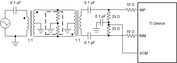
GUID-9C33BCB1-E186-4BE1-805C-68481F7B537D-low.gifFigure 9-7 Driving Circuit for High Input Frequencies (fIN > 230 MHz)