ZHCSDY0A May 2014 – June 2015 ADC32J22 , ADC32J23 , ADC32J24 , ADC32J25
PRODUCTION DATA.
- 1 特性
- 2 应用
- 3 说明
- 4 修订历史记录
- 5 Device Comparison Table
- 6 Pin Configuration and Functions
-
7 Specifications
- 7.1 Absolute Maximum Ratings
- 7.2 ESD Ratings
- 7.3 Recommended Operating Conditions
- 7.4 Thermal Information
- 7.5 Electrical Characteristics
- 7.6 Electrical Characteristics: ADC32J22, ADC32J23
- 7.7 Electrical Characteristics: ADC32J24, ADC32J25
- 7.8 AC Performance: ADC32J25
- 7.9 AC Performance: ADC32J24
- 7.10 AC Performance: ADC32J23
- 7.11 AC Performance: ADC32J22
- 7.12 Digital Characteristics
- 7.13 Timing Requirements
- 7.14 Typical Characteristics: ADC32J25
- 7.15 Typical Characteristics: ADC32J24
- 7.16 Typical Characteristics: ADC32J23
- 7.17 Typical Characteristics: ADC32J22
- 7.18 Typical Characteristics: Common Plots
- 7.19 Typical Characteristics: Contour Plots
- 8 Parameter Measurement Information
-
9 Detailed Description
- 9.1 Overview
- 9.2 Functional Block Diagram
- 9.3 Feature Description
- 9.4 Device Functional Modes
- 9.5 Programming
- 9.6
Register Maps
- 9.6.1 Summary of Special Mode Registers
- 9.6.2
Serial Register Descriptions
- 9.6.2.1 Register 01h (address = 01h)
- 9.6.2.2 Register 03h (address = 03h)
- 9.6.2.3 Register 04h (address = 04h)
- 9.6.2.4 Register 06h (address = 06h)
- 9.6.2.5 Register 07h (address = 07h)
- 9.6.2.6 Register 08h (address = 08h)
- 9.6.2.7 Register 09h (address = 09h)
- 9.6.2.8 Register 0Ah (address = 0Ah)
- 9.6.2.9 Register 0Bh (address = 0Bh)
- 9.6.2.10 Register 0Ch (address = 0Ch)
- 9.6.2.11 Register 0Dh (address = 0Dh)
- 9.6.2.12 Register 0Eh (address = 0Eh)
- 9.6.2.13 Register 0Fh (address = 0Fh)
- 9.6.2.14 Register 13h (address = 13h)
- 9.6.2.15 Register 15h (address = 15h)
- 9.6.2.16 Register 27h (address = 27h)
- 9.6.2.17 Register 2Ah (address = 2Ah)
- 9.6.2.18 Register 2Bh (address = 2Bh)
- 9.6.2.19 Register 2Fh (address = 2Fh)
- 9.6.2.20 Register 30h (address = 30h)
- 9.6.2.21 Register 31h (address = 31h)
- 9.6.2.22 Register 34h (address = 34h)
- 9.6.2.23 Register 3Ah (address = 3Ah)
- 9.6.2.24 Register 3Bh (address = 3Bh)
- 9.6.2.25 Register 3Ch (address = 3Ch)
- 9.6.2.26 Register 422h (address = 422h)
- 9.6.2.27 Register 434h (address = 434h)
- 9.6.2.28 Register 522h (address = 522h)
- 9.6.2.29 Register 534 (address = 534h)
- 10Applications and Implementation
- 11Power Supply Recommendations
- 12Layout
- 13器件和文档支持
- 14机械、封装和可订购信息
12 Layout
12.1 Layout Guidelines
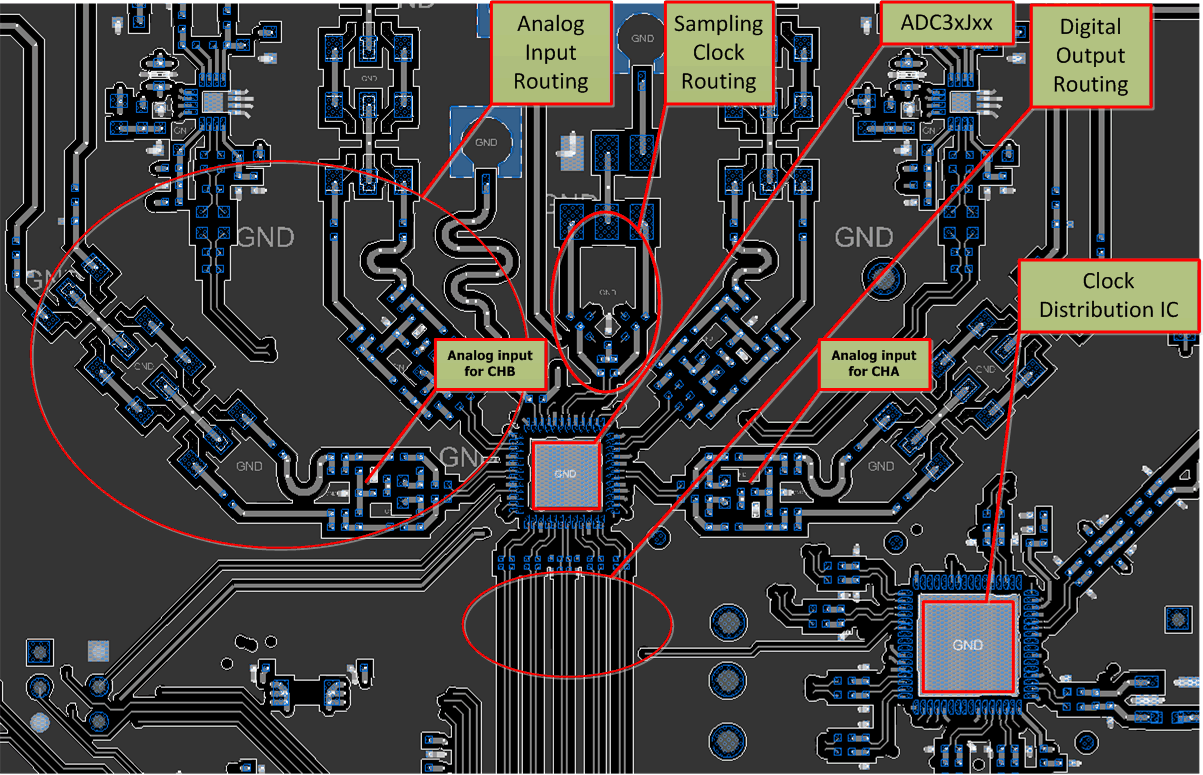
The ADC32J2x EVM layout can be used as a reference layout to obtain the best performance. A layout diagram of the EVM top layer is provided in Figure 202. Some important points to remember when laying out the board are:
- Analog inputs are located on opposite sides of the device pin out to ensure minimum crosstalk on the package level. To minimize crosstalk onboard, the analog inputs must exit the pin out in opposite directions, as shown in the reference layout of Figure 202 as much as possible.
- In the device pin out, the sampling clock is located on a side perpendicular to the analog inputs in order to minimize coupling between them. This configuration is also maintained on the reference layout of Figure 202 as much as possible.
- Keep digital outputs away from the analog inputs. When these digital outputs exit the pin out, the digital output traces must not be kept parallel to the analog input traces because this configuration may result in coupling from digital outputs to analog inputs and degrade performance. All digital output traces to the receiver [such as a field-programmable gate array (FPGA) or an application-specific integrated circuit (ASIC)] must be matched in length to avoid skew among outputs.
- At each power-supply pin (AVDD and DVDD), keep a 0.1-µF decoupling capacitor close to the device. A separate decoupling capacitor group consisting of a parallel combination of 10-µF, 1-µF, and 0.1-µF capacitors can be kept close to the supply source.
12.2 Layout Example
 Figure 202. Typical Layout of the ADC32J2x Board