ZHCSPO2 September 2023 ADC32RF52
PRODUCTION DATA
- 1
- 1 特性
- 2 应用
- 3 说明
- 4 Revision History
- 5 Pin Configuration and Functions
-
6 Specifications
- 6.1 Absolute Maximum Ratings
- 6.2 ESD Ratings
- 6.3 Recommended Operating Conditions
- 6.4 Thermal Information
- 6.5 Electrical Characteristics - Power Consumption
- 6.6 Electrical Characteristics - DC Specifications
- 6.7 Electrical Characteristics - AC Specifications (Dither DISABLED)
- 6.8 Electrical Characteristics - AC Specifications (Dither ENABLED)
- 6.9 Timing Requirements
- 6.10 Typical Characteristics
-
7 Detailed Description
- 7.1 Overview
- 7.2 功能方框图
- 7.3
Feature Description
- 7.3.1 Analog Inputs
- 7.3.2 Sampling Clock Input
- 7.3.3 SYSREF
- 7.3.4 ADC Foreground Calibration
- 7.3.5 Decimation Filter
- 7.3.6
JESD204B Interface
- 7.3.6.1 JESD204B Initial Lane Alignment (ILA)
- 7.3.6.2 JESD204B Frame Assembly
- 7.3.6.3 JESD204B Frame Assembly in Bypass Mode
- 7.3.6.4 JESD204B Frame Assembly with Complex Decimation - Single Band
- 7.3.6.5 JESD204B Frame Assembly with Complex Decimation - Dual Band
- 7.3.6.6 JESD204B Frame Assembly with Complex Decimation - Quad Band
- 7.3.7 SERDES Output MUX
- 7.3.8 Test Pattern
- 7.4 Device Functional Modes
- 7.5 Programming
- 7.6 Register Maps
-
8 Application and Implementation
- 8.1 Application Information
- 8.2 Typical Applications
- 8.3
Initialization Set Up
- 8.3.1
Initial Device Configuration After Power-Up
- 8.3.1.1 STEP 1: RESET
- 8.3.1.2 STEP 2: Device Configuration
- 8.3.1.3 STEP 3: JESD Interface Configuration (1)
- 8.3.1.4 STEP 4: SYSREF Synchronization
- 8.3.1.5 STEP 5: JESD Interface Configuration (2)
- 8.3.1.6 STEP 6: Analog Trim Settings
- 8.3.1.7 STEP 7: Calibration Configuration
- 8.3.1.8 STEP 8: SYSREF Synchronization
- 8.3.1.9 STEP 9: Run Power up Calibration
- 8.3.1.10 STEP 10: JESD Interface Synchronization
- 8.3.1
Initial Device Configuration After Power-Up
- 8.4 Power Supply Recommendations
- 8.5 Layout
- 9 Device and Documentation Support
- 10Mechanical, Packaging, and Orderable Information
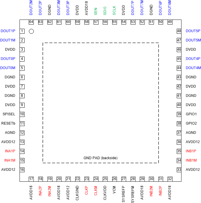
5 Pin Configuration and Functions
 Figure 5-1 RTD (VQFNP) Package, 64 Pin
(Top View)
Table 5-1 Pin Functions
| PIN | TYPE | DESCRIPTION | |
|---|---|---|---|
| NAME | NO. | ||
| Analog Inputs | |||
| INA1P | 14 | I | Differential analog input for channel A. 100 Ω (default) or 50 Ω differential internal termination. |
| INA1M | 15 | ||
| INA2P | 18 | I | Differential analog input for alternate channel A input. This input is used for additional ADC averaging for channel A. 100 Ω (default) or 50 Ω differential internal termination. Should be connected to GND if unused. |
| INA2M | 19 | ||
| INB1P | 35 | I | Differential analog input for channel B. 100 Ω (default) or 50 Ω differential internal termination. |
| INB1M | 34 | ||
| INB2P | 31 | I | Differential analog input for alternate channel B input. This input is used for additional ADC averaging for channel B. 100 Ω (default) or 50 Ω differential internal termination. Should be connected to GND if unused. |
| INB2M | 30 | ||
| VCM | 26 | O | Common-mode voltage output for the analog inputs. |
| Clock, Synchronization | |||
| CLKP | 23 | I | Differential sampling clock input. 100 Ω differential internal termination. |
| CLKM | 24 | ||
| SYSREFP | 27 | I | Differential external synchronization input. |
| SYSREFM | 28 | ||
| Control | |||
| RESETb | 11 | I | Hardware reset. Active low. This pin has an internal 21 kΩ pullup resistor to AVDD18. |
| SEN | 57 | I | Serial interface enable. Active low. This pin has an internal 21 kΩ pull-up resistor to AVDD18. |
| SCLK | 55 | I | Serial interface clock input. This pin has an internal 21 kΩ pull-down resistor. |
| SDIO | 56 | I/O | Serial interface data input and output. This pin has an internal 21 kΩ pull-down resistor. |
| GPIO1 | 39 | I | GPIO control pin. This pin is configured through SPI interface for power down or NCO control function. |
| GPIO2 | 38 | I | GPIO control pin. This pin is configured through SPI interface for power down or NCO control function. |
| SPISEL | 10 | I | Determines SPI control: either normal SPI for register writes or fast access to NCO selection only for fast frequency hopping. |
| Digital Data Interface | |||
| DOUT0P | 4 | O | JESD204B high-speed serial data output interface pins for channel A. |
| DOUT0M | 5 | ||
| DOUT1P | 1 | ||
| DOUT1M | 2 | ||
| DOUT2P | 63 | ||
| DOUT2M | 64 | ||
| DOUT3P | 60 | ||
| DOUT3M | 61 | ||
| DOUT4P | 45 | O | JESD204B high-speed serial data output interface pins for channel B. |
| DOUT4M | 44 | ||
| DOUT5P | 48 | ||
| DOUT5M | 47 | ||
| DOUT6P | 50 | ||
| DOUT6M | 49 | ||
| DOUT7P | 53 | ||
| DOUT7M | 52 | ||
| Power Supply | |||
| AVDD18 | 17,20,29,32, 58 | I | Analog 1.8-V power supply |
| AVDD12 | 13,16,21,33, 36 | I | Analog 1.2-V power supply |
| CLKVDD | 25 | I | Clock 1.2-V power supply. Very sensitive to power supply noise. Directly impacts close in aperture phase noise. |
| DVDD | 3,7,9,40,42, 46,54,59 | I | Digital 1.2-V power supply |
| AGND | 12,37 | I | Analog ground, shorted to thermal pad. |
| CLKGND | 22 | I | Clock ground. |
| DGND | 6,8,41,43,51,62 | I | Digital ground. |