ZHCSPO2 September 2023 ADC32RF52
PRODUCTION DATA
- 1
- 1 特性
- 2 应用
- 3 说明
- 4 Revision History
- 5 Pin Configuration and Functions
-
6 Specifications
- 6.1 Absolute Maximum Ratings
- 6.2 ESD Ratings
- 6.3 Recommended Operating Conditions
- 6.4 Thermal Information
- 6.5 Electrical Characteristics - Power Consumption
- 6.6 Electrical Characteristics - DC Specifications
- 6.7 Electrical Characteristics - AC Specifications (Dither DISABLED)
- 6.8 Electrical Characteristics - AC Specifications (Dither ENABLED)
- 6.9 Timing Requirements
- 6.10 Typical Characteristics
-
7 Detailed Description
- 7.1 Overview
- 7.2 功能方框图
- 7.3
Feature Description
- 7.3.1 Analog Inputs
- 7.3.2 Sampling Clock Input
- 7.3.3 SYSREF
- 7.3.4 ADC Foreground Calibration
- 7.3.5 Decimation Filter
- 7.3.6
JESD204B Interface
- 7.3.6.1 JESD204B Initial Lane Alignment (ILA)
- 7.3.6.2 JESD204B Frame Assembly
- 7.3.6.3 JESD204B Frame Assembly in Bypass Mode
- 7.3.6.4 JESD204B Frame Assembly with Complex Decimation - Single Band
- 7.3.6.5 JESD204B Frame Assembly with Complex Decimation - Dual Band
- 7.3.6.6 JESD204B Frame Assembly with Complex Decimation - Quad Band
- 7.3.7 SERDES Output MUX
- 7.3.8 Test Pattern
- 7.4 Device Functional Modes
- 7.5 Programming
- 7.6 Register Maps
-
8 Application and Implementation
- 8.1 Application Information
- 8.2 Typical Applications
- 8.3
Initialization Set Up
- 8.3.1
Initial Device Configuration After Power-Up
- 8.3.1.1 STEP 1: RESET
- 8.3.1.2 STEP 2: Device Configuration
- 8.3.1.3 STEP 3: JESD Interface Configuration (1)
- 8.3.1.4 STEP 4: SYSREF Synchronization
- 8.3.1.5 STEP 5: JESD Interface Configuration (2)
- 8.3.1.6 STEP 6: Analog Trim Settings
- 8.3.1.7 STEP 7: Calibration Configuration
- 8.3.1.8 STEP 8: SYSREF Synchronization
- 8.3.1.9 STEP 9: Run Power up Calibration
- 8.3.1.10 STEP 10: JESD Interface Synchronization
- 8.3.1
Initial Device Configuration After Power-Up
- 8.4 Power Supply Recommendations
- 8.5 Layout
- 9 Device and Documentation Support
- 10Mechanical, Packaging, and Orderable Information
7.3.3.1 SYSREF Capture Detection
The SYSREF input signal rising edge should be edge aligned with the rising edge of the sampling clock to maximize the setup and hold times. The ADC32RF52 includes an internal SYSREF monitoring circuitry to detect possible metastability resulting in a clock cycle slip; and thus, misalignment across devices.
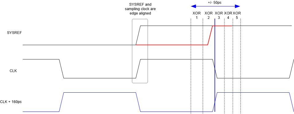
The sampling clock gets delayed by ~160 ps and then captures the SYSREF signal. The SYSREF monitoring circuitry captures the SYSREF signal ±50 ps (-50, -25, +16, +32, +48 ps) around the main SYSREF capture. In ideal conditions no SYSREF transition happens within the 100 ps SYSREF capture window and all XOR flags show "0". If a SYSREF/clock misalignment happens and the SYSREF transition falls within the SYSREF monitoring window, then one of the XOR flags (which monitor adjacent SYSREF captures within the window) shows a "1" and the SYSREF can be adjusted externally.
The SYSREF monitor registers are not 'sticky' registers - they get updated at every rising edge of SYSREF.
 Figure 7-13 SYSREF Detection Circuitry
The example in Figure 7-14 shows a misaligned SYSREF signal where the SYSREF signal arrives much later than the sampling clock rising edge. The SYSREF window feature checks if the SYSREF transition is within ±50 ps of the instant when the SYSREF signal gets captured by the sampling clock.
In this example, the delayed SYSREF signal transitions between the "B" and "C" flip flop which raises the XOR2 flag. The XOR flags get reported in register 0x22F in the digital page. In this exampe, Register 0x22F reads back 0x8B, as shown in Table 7-11.
 Figure 7-14 Detection of SYSREF Transition within Capture Window
| ADDR | D7 | D6 | D5 | D4 | D3 | D2 | D1 | D0 |
|---|---|---|---|---|---|---|---|---|
| 0x22F | 1 | SYSREF X5 | SYSREF X4 | SYSREF X3 | SYSREF X2 | SYSREF X1 | SYSREF OR | 1 |
| 1 | 0 | 0 | 0 | 1 | 0 | 1 | 1 |