ZHCSFU8B May 2016 – December 2021 ADC32RF80 , ADC32RF83
PRODUCTION DATA
- 1 特性
- 2 应用
- 3 说明
- 4 Revision History
- 5 Pin Configuration and Functions
-
6 Specifications
- 6.1 Absolute Maximum Ratings
- 6.2 ESD Ratings
- 6.3 Recommended Operating Conditions
- 6.4 Thermal Information
- 6.5 Electrical Characteristics
- 6.6 AC Performance Characteristics: fS = 2949.12 MSPS
- 6.7 AC Performance Characteristics: fS = 2457.6 MSPS (Performance Optimized for F + A + D Band)
- 6.8 AC Performance Characteristics: fS = 2457.6 MSPS (Performance Optimized for F + A Band)
- 6.9 Digital Requirements
- 6.10 Timing Requirements
- 6.11 Typical Characteristics
- 7 Parameter Measurement Information
-
8 Detailed Description
- 8.1 Overview
- 8.2 Functional Block Diagram
- 8.3
Feature Description
- 8.3.1 Analog Inputs
- 8.3.2 Clock Input
- 8.3.3 SYSREF Input
- 8.3.4 DDC Block
- 8.3.5 NCO Switching
- 8.3.6 SerDes Transmitter Interface
- 8.3.7 Eye Diagrams
- 8.3.8 Alarm Outputs: Power Detectors for AGC Support
- 8.3.9 Power-Down Mode
- 8.3.10 ADC Test Pattern
- 8.4
Device Functional Modes
- 8.4.1 Device Configuration
- 8.4.2
JESD204B Interface
- 8.4.2.1 JESD204B Initial Lane Alignment (ILA)
- 8.4.2.2 JESD204B Frame Assembly
- 8.4.2.3 JESD204B Frame Assembly with Decimation (Single-Band DDC): Complex Output
- 8.4.2.4 JESD204B Frame Assembly with Decimation (Single-Band DDC): Real Output
- 8.4.2.5 JESD204B Frame Assembly with Decimation (Single-Band DDC): Real Output
- 8.4.2.6 JESD204B Frame Assembly with Decimation (Dual-Band DDC): Complex Output
- 8.4.2.7 JESD204B Frame Assembly with Decimation (Dual-Band DDC): Real Output
- 8.4.3 Serial Interface
- 8.5
Register Maps
- 8.5.1 Example Register Writes
- 8.5.2
Register Descriptions
- 8.5.2.1
General Registers
- 8.5.2.1.1 Register 000h (address = 000h), General Registers
- 8.5.2.1.2 Register 002h (address = 002h), General Registers
- 8.5.2.1.3 Register 003h (address = 003h), General Registers
- 8.5.2.1.4 Register 004h (address = 004h), General Registers
- 8.5.2.1.5 Register 010h (address = 010h), General Registers
- 8.5.2.1.6 Register 011h (address = 011h), General Registers
- 8.5.2.1.7 Register 012h (address = 012h), General Registers
- 8.5.2.1
General Registers
- 8.5.3
Master Page (M = 0)
- 8.5.3.1 Register 020h (address = 020h), Master Page
- 8.5.3.2 Register 032h (address = 032h), Master Page
- 8.5.3.3 Register 039h (address = 039h), Master Page
- 8.5.3.4 Register 03Ch (address = 03Ch), Master Page
- 8.5.3.5 Register 05Ah (address = 05Ah), Master Page
- 8.5.3.6 Register 03Dh (address = 3Dh), Master Page
- 8.5.3.7 Register 057h (address = 057h), Master Page
- 8.5.3.8 Register 058h (address = 058h), Master Page
- 8.5.4 ADC Page (FFh, M = 0)
- 8.5.5 Digital Function Page (610000h, M = 1 for Channel A and 610100h, M = 1 for Channel B)
- 8.5.6 Offset Corr Page Channel A (610000h, M = 1)
- 8.5.7 Offset Corr Page Channel B (610000h, M = 1)
- 8.5.8 Digital Gain Page (610005h, M = 1 for Channel A and 610105h, M = 1 for Channel B)
- 8.5.9 Main Digital Page Channel A (680000h, M = 1)
- 8.5.10 Main Digital Page Channel B (680001h, M = 1)
- 8.5.11
JESD Digital Page (6900h, M = 1)
- 8.5.11.1 Register 001h (address = 001h), JESD Digital Page
- 8.5.11.2 Register 002h (address = 002h ), JESD Digital Page
- 8.5.11.3 Register 003h (address = 003h), JESD Digital Page
- 8.5.11.4 Register 004h (address = 004h), JESD Digital Page
- 8.5.11.5 Register 006h (address = 006h), JESD Digital Page
- 8.5.11.6 Register 007h (address = 007h), JESD Digital Page
- 8.5.11.7 Register 016h (address = 016h), JESD Digital Page
- 8.5.11.8 Register 017h (address = 017h), JESD Digital Page
- 8.5.11.9 Register 032h-035h (address = 032h-035h), JESD Digital Page
- 8.5.11.10 Register 036h (address = 036h), JESD Digital Page
- 8.5.11.11 Register 037h (address = 037h), JESD Digital Page
- 8.5.11.12 Register 03Ch (address = 03Ch), JESD Digital Page
- 8.5.11.13 Register 03Eh (address = 03Eh), JESD Digital Page
- 8.5.12
Decimation Filter Page
- 8.5.12.1 Register 000h (address = 000h), Decimation Filter Page
- 8.5.12.2 Register 001h (address = 001h), Decimation Filter Page
- 8.5.12.3 Register 002h (address = 2h), Decimation Filter Page
- 8.5.12.4 Register 005h (address = 005h), Decimation Filter Page
- 8.5.12.5 Register 006h (address = 006h), Decimation Filter Page
- 8.5.12.6 Register 007h (address = 007h), Decimation Filter Page
- 8.5.12.7 Register 008h (address = 008h), Decimation Filter Page
- 8.5.12.8 Register 009h (address = 009h), Decimation Filter Page
- 8.5.12.9 Register 00Ah (address = 00Ah), Decimation Filter Page
- 8.5.12.10 Register 00Bh (address = 00Bh), Decimation Filter Page
- 8.5.12.11 Register 00Ch (address = 00Ch), Decimation Filter Page
- 8.5.12.12 Register 00Dh (address = 00Dh), Decimation Filter Page
- 8.5.12.13 Register 00Eh (address = 00Eh), Decimation Filter Page
- 8.5.12.14 Register 00Fh (address = 00Fh), Decimation Filter Page
- 8.5.12.15 Register 010h (address = 010h), Decimation Filter Page
- 8.5.12.16 Register 011h (address = 011h), Decimation Filter Page
- 8.5.12.17 Register 014h (address = 014h), Decimation Filter Page
- 8.5.12.18 Register 016h (address = 016h), Decimation Filter Page
- 8.5.12.19 Register 01Eh (address = 01Eh), Decimation Filter Page
- 8.5.12.20 Register 01Fh (address = 01Fh), Decimation Filter Page
- 8.5.12.21 Register 033h-036h (address = 033h-036h), Decimation Filter Page
- 8.5.12.22 Register 037h (address = 037h), Decimation Filter Page
- 8.5.12.23 Register 03Ah (address = 03Ah), Decimation Filter Page
- 8.5.13
Power Detector Page
- 8.5.13.1 Register 000h (address = 000h), Power Detector Page
- 8.5.13.2 Register 001h-002h (address = 001h-002h), Power Detector Page
- 8.5.13.3 Register 003h (address = 003h), Power Detector Page
- 8.5.13.4 Register 007h-00Ah (address = 007h-00Ah), Power Detector Page
- 8.5.13.5 Register 00Bh-00Ch (address = 00Bh-00Ch), Power Detector Page
- 8.5.13.6 Register 00Dh (address = 00Dh), Power Detector Page
- 8.5.13.7 Register 00Eh (address = 00Eh), Power Detector Page
- 8.5.13.8 Register 00Fh, 010h-012h, and 016h-019h (address = 00Fh, 010h-012h, and 016h-019h), Power Detector Page
- 8.5.13.9 Register 013h-01Ah (address = 013h-01Ah), Power Detector Page
- 8.5.13.10 Register 01Dh-01Eh (address = 01Dh-01Eh), Power Detector Page
- 8.5.13.11 Register 020h (address = 020h), Power Detector Page
- 8.5.13.12 Register 021h (address = 021h), Power Detector Page
- 8.5.13.13 Register 022h-025h (address = 022h-025h), Power Detector Page
- 8.5.13.14 Register 027h (address = 027h), Power Detector Page
- 8.5.13.15 Register 02Bh (address = 02Bh), Power Detector Page
- 8.5.13.16 Register 032h-035h (address = 032h-035h), Power Detector Page
- 8.5.13.17 Register 037h (address = 037h), Power Detector Page
- 8.5.13.18 Register 038h (address = 038h), Power Detector Page
- 9 Application and Implementation
- 10Power Supply Recommendations
- 11Layout
- 12Device and Documentation Support
- 13Mechanical, Packaging, and Orderable Information
9.1.3.1 External Clock Phase Noise Consideration
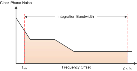
External clock jitter can be calculated by integrating the phase noise of the clock source out to approximately two times of the ADC sampling rate (2 × fS), as shown in Figure 9-3. In order to maximize the ADC SNR, an external band-pass filter is recommended to be used on the clock input. This filter reduces the jitter contribution from the broadband clock phase noise floor by effectively reducing the integration bandwidth to the pass band of the band-pass filter. This method is suitable when estimating the overall ADC SNR resulting from clock jitter at a certain input frequency.
 Figure 9-3 Integration Bandwidth for Extracting Jitter from Clock Phase Noise
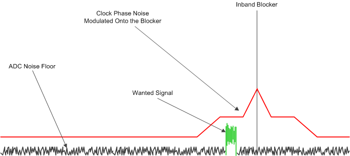
However, when estimating the affect of a nearby blocker (such as a strong in-band interferer to the sensitivity, the phase noise information can be used directly to estimate the noise budget contribution at a certain offset frequency, as shown in Figure 9-4.
 Figure 9-4 Small Wanted Signal in Presence of Interferer
At the sampling instant, the phase noise profile of the clock source convolves with the input signal (for example, the small wanted signal and the strong interferer merge together). If the power of the clock phase noise in the signal band of interest is too large, the wanted signal cannot not be recovered.
The resulting equivalent phase noise at the ADC input is also dependent on the sampling rate of the ADC and frequency of the input signal. The ADC sampling rate scales the clock phase noise, as shown in Equation 8.

Using this information, the noise contribution resulting from the phase noise profile of the ADC sampling clock can be calculated.