ZHCSFU8B May   2016  – December 2021 ADC32RF80 , ADC32RF83

PRODUCTION DATA  

  1. 特性
  2. 应用
  3. 说明
  4. Revision History
  5. Pin Configuration and Functions
  6. Specifications
    1. 6.1  Absolute Maximum Ratings
    2. 6.2  ESD Ratings
    3. 6.3  Recommended Operating Conditions
    4. 6.4  Thermal Information
    5. 6.5  Electrical Characteristics
    6. 6.6  AC Performance Characteristics: fS = 2949.12 MSPS
    7. 6.7  AC Performance Characteristics: fS = 2457.6 MSPS (Performance Optimized for F + A + D Band)
    8. 6.8  AC Performance Characteristics: fS = 2457.6 MSPS (Performance Optimized for F + A Band)
    9. 6.9  Digital Requirements
    10. 6.10 Timing Requirements
    11. 6.11 Typical Characteristics
  7. Parameter Measurement Information
    1. 7.1 Input Clock Diagram
  8. Detailed Description
    1. 8.1 Overview
    2. 8.2 Functional Block Diagram
    3. 8.3 Feature Description
      1. 8.3.1  Analog Inputs
        1. 8.3.1.1 Input Clamp Circuit
      2. 8.3.2  Clock Input
      3. 8.3.3  SYSREF Input
        1. 8.3.3.1 Using SYSREF
        2. 8.3.3.2 Frequency of the SYSREF Signal
      4. 8.3.4  DDC Block
        1. 8.3.4.1 Operating Mode: Receiver
        2. 8.3.4.2 Operating Mode: Wide-Bandwidth Observation Receiver
        3. 8.3.4.3 Decimation Filters
          1. 8.3.4.3.1  Divide-by-4
          2. 8.3.4.3.2  Divide-by-6
          3. 8.3.4.3.3  Divide-by-8
          4. 8.3.4.3.4  Divide-by-9
          5. 8.3.4.3.5  Divide-by-10
          6. 8.3.4.3.6  Divide-by-12
          7. 8.3.4.3.7  Divide-by-16
          8. 8.3.4.3.8  Divide-by-18
          9. 8.3.4.3.9  Divide-by-20
          10. 8.3.4.3.10 Divide-by-24
          11. 8.3.4.3.11 Divide-by-32
          12. 8.3.4.3.12 Latency with Decimation Options
        4. 8.3.4.4 Digital Multiplexer (MUX)
        5. 8.3.4.5 Numerically-Controlled Oscillators (NCOs) and Mixers
      5. 8.3.5  NCO Switching
      6. 8.3.6  SerDes Transmitter Interface
      7. 8.3.7  Eye Diagrams
      8. 8.3.8  Alarm Outputs: Power Detectors for AGC Support
        1. 8.3.8.1 Absolute Peak Power Detector
        2. 8.3.8.2 Crossing Detector
        3. 8.3.8.3 RMS Power Detector
        4. 8.3.8.4 GPIO AGC MUX
      9. 8.3.9  Power-Down Mode
      10. 8.3.10 ADC Test Pattern
        1. 8.3.10.1 Digital Block
        2. 8.3.10.2 Transport Layer
        3. 8.3.10.3 Link Layer
    4. 8.4 Device Functional Modes
      1. 8.4.1 Device Configuration
      2. 8.4.2 JESD204B Interface
        1. 8.4.2.1 JESD204B Initial Lane Alignment (ILA)
        2. 8.4.2.2 JESD204B Frame Assembly
        3. 8.4.2.3 JESD204B Frame Assembly with Decimation (Single-Band DDC): Complex Output
        4. 8.4.2.4 JESD204B Frame Assembly with Decimation (Single-Band DDC): Real Output
        5. 8.4.2.5 JESD204B Frame Assembly with Decimation (Single-Band DDC): Real Output
        6. 8.4.2.6 JESD204B Frame Assembly with Decimation (Dual-Band DDC): Complex Output
        7. 8.4.2.7 JESD204B Frame Assembly with Decimation (Dual-Band DDC): Real Output
      3. 8.4.3 Serial Interface
        1. 8.4.3.1 Serial Register Write: Analog Bank
        2. 8.4.3.2 Serial Register Readout: Analog Bank
        3. 8.4.3.3 Serial Register Write: Digital Bank
        4. 8.4.3.4 Serial Register Readout: Digital Bank
        5. 8.4.3.5 Serial Register Write: Decimation Filter and Power Detector Pages
    5. 8.5 Register Maps
      1. 8.5.1  Example Register Writes
      2. 8.5.2  Register Descriptions
        1. 8.5.2.1 General Registers
          1. 8.5.2.1.1 Register 000h (address = 000h), General Registers
          2. 8.5.2.1.2 Register 002h (address = 002h), General Registers
          3. 8.5.2.1.3 Register 003h (address = 003h), General Registers
          4. 8.5.2.1.4 Register 004h (address = 004h), General Registers
          5. 8.5.2.1.5 Register 010h (address = 010h), General Registers
          6. 8.5.2.1.6 Register 011h (address = 011h), General Registers
          7. 8.5.2.1.7 Register 012h (address = 012h), General Registers
      3. 8.5.3  Master Page (M = 0)
        1. 8.5.3.1 Register 020h (address = 020h), Master Page
        2. 8.5.3.2 Register 032h (address = 032h), Master Page
        3. 8.5.3.3 Register 039h (address = 039h), Master Page
        4. 8.5.3.4 Register 03Ch (address = 03Ch), Master Page
        5. 8.5.3.5 Register 05Ah (address = 05Ah), Master Page
        6. 8.5.3.6 Register 03Dh (address = 3Dh), Master Page
        7. 8.5.3.7 Register 057h (address = 057h), Master Page
        8. 8.5.3.8 Register 058h (address = 058h), Master Page
      4. 8.5.4  ADC Page (FFh, M = 0)
        1. 8.5.4.1 Register 03Fh (address = 03Fh), ADC Page
        2. 8.5.4.2 Register 042h (address = 042h), ADC Page
      5. 8.5.5  Digital Function Page (610000h, M = 1 for Channel A and 610100h, M = 1 for Channel B)
        1. 8.5.5.1 Register A6h (address = 0A6h), Digital Function Page
      6. 8.5.6  Offset Corr Page Channel A (610000h, M = 1)
        1. 8.5.6.1 Register 034h (address = 034h), Offset Corr Page Channel A
        2. 8.5.6.2 Register 068h (address = 068h), Offset Corr Page Channel A
      7. 8.5.7  Offset Corr Page Channel B (610000h, M = 1)
        1. 8.5.7.1 Register 068h (address = 068h), Offset Corr Page Channel B
      8. 8.5.8  Digital Gain Page (610005h, M = 1 for Channel A and 610105h, M = 1 for Channel B)
        1. 8.5.8.1 Register 0A6h (address = 0A6h), Digital Gain Page
      9. 8.5.9  Main Digital Page Channel A (680000h, M = 1)
        1. 8.5.9.1 Register 000h (address = 000h), Main Digital Page Channel A
        2. 8.5.9.2 Register 0A2h (address = 0A2h), Main Digital Page Channel A
      10. 8.5.10 Main Digital Page Channel B (680001h, M = 1)
        1. 8.5.10.1 Register 000h (address = 000h), Main Digital Page Channel B
        2. 8.5.10.2 Register 0A2h (address = 0A2h), Main Digital Page Channel B
      11. 8.5.11 JESD Digital Page (6900h, M = 1)
        1. 8.5.11.1  Register 001h (address = 001h), JESD Digital Page
        2. 8.5.11.2  Register 002h (address = 002h ), JESD Digital Page
        3. 8.5.11.3  Register 003h (address = 003h), JESD Digital Page
        4. 8.5.11.4  Register 004h (address = 004h), JESD Digital Page
        5. 8.5.11.5  Register 006h (address = 006h), JESD Digital Page
        6. 8.5.11.6  Register 007h (address = 007h), JESD Digital Page
        7. 8.5.11.7  Register 016h (address = 016h), JESD Digital Page
        8. 8.5.11.8  Register 017h (address = 017h), JESD Digital Page
        9. 8.5.11.9  Register 032h-035h (address = 032h-035h), JESD Digital Page
        10. 8.5.11.10 Register 036h (address = 036h), JESD Digital Page
        11. 8.5.11.11 Register 037h (address = 037h), JESD Digital Page
        12. 8.5.11.12 Register 03Ch (address = 03Ch), JESD Digital Page
        13. 8.5.11.13 Register 03Eh (address = 03Eh), JESD Digital Page
      12. 8.5.12 Decimation Filter Page
        1. 8.5.12.1  Register 000h (address = 000h), Decimation Filter Page
        2. 8.5.12.2  Register 001h (address = 001h), Decimation Filter Page
        3. 8.5.12.3  Register 002h (address = 2h), Decimation Filter Page
        4. 8.5.12.4  Register 005h (address = 005h), Decimation Filter Page
        5. 8.5.12.5  Register 006h (address = 006h), Decimation Filter Page
        6. 8.5.12.6  Register 007h (address = 007h), Decimation Filter Page
        7. 8.5.12.7  Register 008h (address = 008h), Decimation Filter Page
        8. 8.5.12.8  Register 009h (address = 009h), Decimation Filter Page
        9. 8.5.12.9  Register 00Ah (address = 00Ah), Decimation Filter Page
        10. 8.5.12.10 Register 00Bh (address = 00Bh), Decimation Filter Page
        11. 8.5.12.11 Register 00Ch (address = 00Ch), Decimation Filter Page
        12. 8.5.12.12 Register 00Dh (address = 00Dh), Decimation Filter Page
        13. 8.5.12.13 Register 00Eh (address = 00Eh), Decimation Filter Page
        14. 8.5.12.14 Register 00Fh (address = 00Fh), Decimation Filter Page
        15. 8.5.12.15 Register 010h (address = 010h), Decimation Filter Page
        16. 8.5.12.16 Register 011h (address = 011h), Decimation Filter Page
        17. 8.5.12.17 Register 014h (address = 014h), Decimation Filter Page
        18. 8.5.12.18 Register 016h (address = 016h), Decimation Filter Page
        19. 8.5.12.19 Register 01Eh (address = 01Eh), Decimation Filter Page
        20. 8.5.12.20 Register 01Fh (address = 01Fh), Decimation Filter Page
        21. 8.5.12.21 Register 033h-036h (address = 033h-036h), Decimation Filter Page
        22. 8.5.12.22 Register 037h (address = 037h), Decimation Filter Page
          1. 8.5.12.22.1 Register 038h (address = 038h), Decimation Filter Page
          2. 8.5.12.22.2 Register 039h (address = 039h), Decimation Filter Page
        23. 8.5.12.23 Register 03Ah (address = 03Ah), Decimation Filter Page
      13. 8.5.13 Power Detector Page
        1. 8.5.13.1  Register 000h (address = 000h), Power Detector Page
        2. 8.5.13.2  Register 001h-002h (address = 001h-002h), Power Detector Page
        3. 8.5.13.3  Register 003h (address = 003h), Power Detector Page
        4. 8.5.13.4  Register 007h-00Ah (address = 007h-00Ah), Power Detector Page
        5. 8.5.13.5  Register 00Bh-00Ch (address = 00Bh-00Ch), Power Detector Page
        6. 8.5.13.6  Register 00Dh (address = 00Dh), Power Detector Page
        7. 8.5.13.7  Register 00Eh (address = 00Eh), Power Detector Page
        8. 8.5.13.8  Register 00Fh, 010h-012h, and 016h-019h (address = 00Fh, 010h-012h, and 016h-019h), Power Detector Page
        9. 8.5.13.9  Register 013h-01Ah (address = 013h-01Ah), Power Detector Page
        10. 8.5.13.10 Register 01Dh-01Eh (address = 01Dh-01Eh), Power Detector Page
        11. 8.5.13.11 Register 020h (address = 020h), Power Detector Page
        12. 8.5.13.12 Register 021h (address = 021h), Power Detector Page
        13. 8.5.13.13 Register 022h-025h (address = 022h-025h), Power Detector Page
        14. 8.5.13.14 Register 027h (address = 027h), Power Detector Page
        15. 8.5.13.15 Register 02Bh (address = 02Bh), Power Detector Page
        16. 8.5.13.16 Register 032h-035h (address = 032h-035h), Power Detector Page
        17. 8.5.13.17 Register 037h (address = 037h), Power Detector Page
        18. 8.5.13.18 Register 038h (address = 038h), Power Detector Page
  9. Application and Implementation
    1. 9.1 Application Information
      1. 9.1.1 Start-Up Sequence
      2. 9.1.2 Hardware Reset
      3. 9.1.3 SNR and Clock Jitter
        1. 9.1.3.1 External Clock Phase Noise Consideration
      4. 9.1.4 Power Consumption in Different Modes
      5. 9.1.5 Using DC Coupling in the ADC32RF8x
        1. 9.1.5.1 Bypassing the Offset Corrector Block
          1. 9.1.5.1.1 Effect of Temperature
    2. 9.2 Typical Application
      1. 9.2.1 Design Requirements
        1. 9.2.1.1 Transformer-Coupled Circuits
      2. 9.2.2 Detailed Design Procedure
      3. 9.2.3 Application Curves
  10. 10Power Supply Recommendations
  11. 11Layout
    1. 11.1 Layout Guidelines
    2. 11.2 Layout Example
  12. 12Device and Documentation Support
    1. 12.1 Documentation Support
      1. 12.1.1 Related Documentation
    2. 12.2 接收文档更新通知
    3. 12.3 支持资源
    4. 12.4 Trademarks
    5. 12.5 Electrostatic Discharge Caution
    6. 12.6 术语表
  13. 13Mechanical, Packaging, and Orderable Information

封装选项

机械数据 (封装 | 引脚)
散热焊盘机械数据 (封装 | 引脚)
订购信息

Typical Characteristics

typical values are specified at an ambient temperature of 25°C; minimum and maximum values are specified over an ambient temperature range of –40°C to +85°C; and ADC sampling rate = 2949.12 MSPS, DDC bypassed performance, 50% clock duty cycle, AVDD19 = 1.9 V, AVDD = DVDD = 1.15 V, –2-dBFS differential input, and 0-dB digital gain (unless otherwise noted)
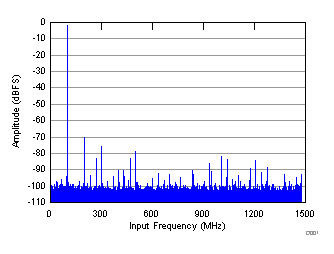
GUID-BB3A738E-366F-43D6-974E-813A99AD1DB6-low.gif
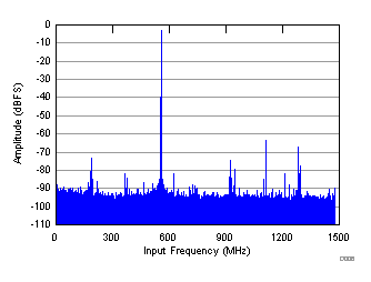
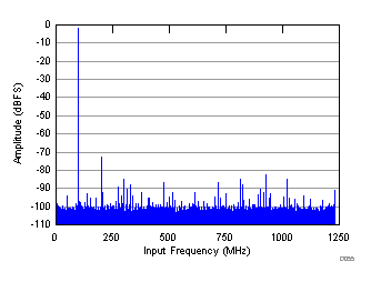
SNR = 62.2 dBFS; SFDR = 68 dBc; HD2 = –68 dBc; HD3 = –73 dBc; non HD2, HD3 = 77 dBc; IL spur = 86 dBc; fIN = 100 MHz
Figure 6-3 FFT for 100-MHz Input Frequency
GUID-6FD0AA8E-A302-4594-B527-B69CC8928965-low.gif
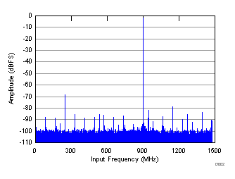
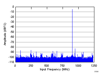
SNR = 61.2 dBFS; SFDR = 66 dBc; HD2 = –77 dBc; HD3 = –66 dBc; non HD2, HD3 = 80 dBc; IL spur = 83 dBc; fIN = 900 MHz
Figure 6-5 FFT for 900-MHz Input Signal
GUID-A05B0E9D-C4D5-4C17-8D76-148ACB054C21-low.gif
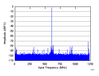
SNR = 59.1 dBFS; SFDR = 65 dBc; HD2 = –65 dBc; HD3 = –73 dBc; non HD2, HD3 = 73 dBc; IL spur = 76 dBc; fIN = 1.7 GHz
Figure 6-7 FFT for 1780-MHz Input Signal
GUID-C6359111-6BEE-47C9-8422-5CB61B6EFD1B-low.gif
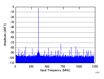
SNR = 58.2 dBFS; SFDR = 64 dBc; HD2 = –64 dBc; HD3 = –85 dBc; non HD2, HD3 = 73 dBc; IL spur = 74 dBc; fIN = 2.1 GHz
Figure 6-9 FFT for 2100-MHz Input Signal
GUID-6AC386A7-6103-4B8A-AE9F-486BE6E8D32C-low.gif
SNR = 56.9 dBFS; SFDR = 62 dBc; HD2 = –62 dBc; HD3 = –72 dBc; non HD2, HD3 = 72 dBc; IL spur = 64 dBc; fIN = 2.6 GHz
Figure 6-11 FFT for 2600-MHz Input Signal
GUID-29306187-281A-4C3E-8972-0475EDEA0F92-low.gif
SNR = 54.2 dBFS; SFDR = 60 dBc; HD2 = –60 dBc; HD3 = –64 dBc; non HD2, HD3 = 71 dBc; IL spur = 80 dBc; fIN = 3.5 GHz, AIN = –3 dBFS with 2-dB gain
Figure 6-13 FFT for 3500-MHz Input Signal
GUID-AE6B0A39-71E5-4C2B-A88B-D9A1E390B5F3-low.gif
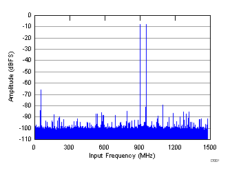
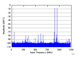
fIN1 = 900 MHz, fIN2 = 950 MHz, AIN = –8 dBFS, IMD = 79 dBFS
Figure 6-15 FFT for Two-Tone Input Signal (–8 dBFS)
GUID-2617B9B5-B952-4EDA-9974-B6FDDC59AAA2-low.gif
fIN1 = 900 MHz, fIN2 = 950 MHz, AIN = –8 dBFS, IMD = 75 dBFS
Figure 6-17 FFT for Two-Tone Input Signal (–8 dBFS, fS = 2457.6 MSPS)
GUID-7E85E13B-1955-49FC-AB77-3E993DAC4FF2-low.gif
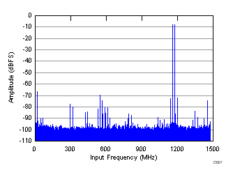
fIN1 = 1.77 GHz, fIN2 = 1.79 GHz, AIN = –8 dBFS, IMD = 70 dBFS
Figure 6-19 FFT for Two-Tone Input Signal (–8 dBFS)
GUID-0E4E961B-F365-4A37-A534-D7C324E08275-low.gif
fIN1 = 1.77 GHz, fIN2 = 1.79 GHz, AIN = –8 dBFS, IMD = 76 dBFS
Figure 6-21 FFT for Two-Tone Input Signal (–8 dBFS, fS = 2457.6 MSPS)
GUID-0E49CF5B-7027-48F4-8435-2ACC61F07353-low.gif
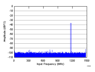
fIN1 = 1.8 MHz, fIN2 = 2.6 GHz, AIN = –8 dBFS, IMD = 71 dBFS
Figure 6-23 FFT for Two-Tone Input Signal (–8 dBFS)
GUID-C97C4172-BD71-41A1-B335-35ECD746C9A5-low.gif
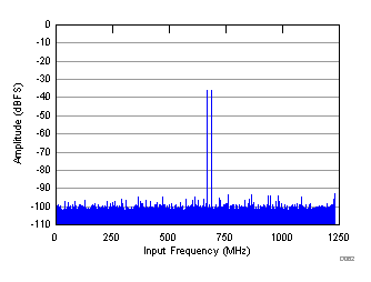
fIN1 = 2.09 GHz, fIN2 = 2.1 GHz, AIN = –8 dBFS, IMD = 76 dBFS
Figure 6-25 FFT for Two-Tone Input Signal (–8 dBFS, fS = 2457.6 MSPS)
GUID-7C648716-6320-4D83-9E22-754C8A535B16-low.gif
fIN1 = 3.49 MHz, fIN2 = 3.51 GHz, IMD = 66 dBFS, AIN = –3 dBFS with 2-dB gain
Figure 6-27 FFT for Two-Tone Input Signal (–8 dBFS)
GUID-99F647D6-2949-485D-9588-9D7629F7D917-low.gif
fIN1 = 2.59 GHz, fIN2 = 2.6 GHz, AIN = –8 dBFS, IMD = 65 dBFS
Figure 6-29 FFT for Two-Tone Input Signal (–8 dBFS, fS = 2457.6 MSPS)
GUID-FA728575-216A-4F1C-AD95-27D672E6A0AD-low.gif
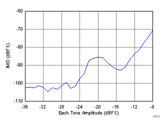
fIN1 = 1.77 GHz, fIN2 = 1.79 GHz
Figure 6-31 Intermodulation Distortion vs. Input Amplitude (1770 MHz and 1790 MHz)
GUID-B182FCAA-92E5-4C4F-A99E-2A59A88B85A9-low.gif
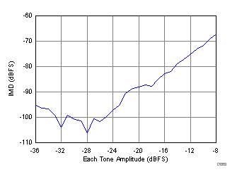
fIN1 = 1.8 GHz, fIN2 = 2.6 GHz, AIN = –36 dBFS
Figure 6-33 Intermodulation Distortion vs. Input Amplitude (1800 MHz and 2600 MHz)
GUID-B7A90E07-85EA-4953-940E-0D2D7A30B8ED-low.gif
fIN1 = 3.49 GHz, fIN2 = 3.51 GHz with 2-dB digital gain
Figure 6-35 Intermodulation Distortion vs. Input Amplitude (3490 MHz and 3510 MHz)
GUID-AF6EA655-07F8-49AE-A463-AF397DB38A75-low.gif
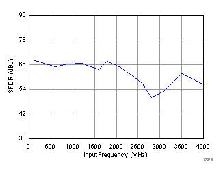
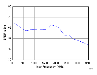
AOUT = –2 dBFS with 0-dB gain for fIN less than 3 GHz, AOUT = –3 dBFS with 2-dB gain for fIN more than 3 GHz
Figure 6-37 Spurious-Free Dynamic Range vs. Input Frequency
GUID-3AB6F45F-68B5-430D-9DB8-28B67394C264-low.gif
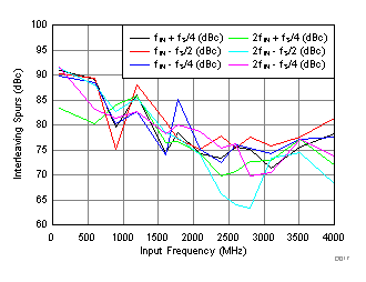
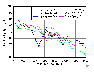
AOUT = –2 dBFS with 0-dB gain for fIN less than 3 GHz, AOUT = –3 dBFS with 2-dB gain for fIN more than 3 GHz
Figure 6-39 IL Spur vs. Input Frequency
GUID-54811725-5C0A-45F9-AB42-58F97970AAC3-low.gif
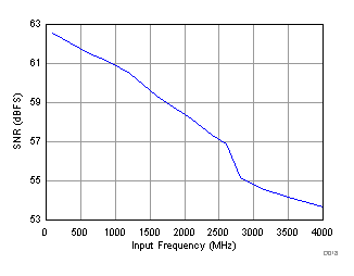
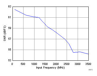
AOUT = –2 dBFS with 0-dB gain for fIN less than 3 GHz, AOUT = –3 dBFS with 2-dB gain for fIN more than 3 GHz
Figure 6-41 Signal-to-Noise Ratio vs. Input Frequency
GUID-C554431D-FB76-4FB0-B765-0D08639D7CA8-low.gif
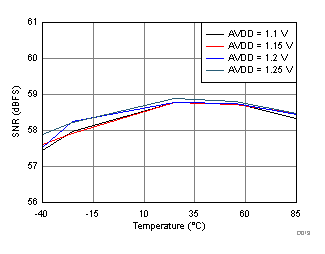
fIN = 1.78 GHz, AIN = –2 dBFS
Figure 6-43 Signal-to-Noise Ratio vs. AVDD Supply and Temperature
GUID-6FCC2FD5-4014-4ADD-BD63-F5FEB2DFA1C0-low.gif
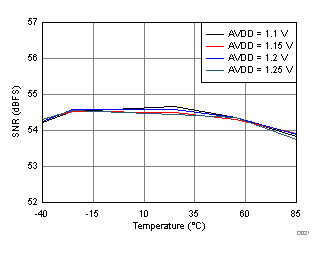
fIN = 3.5 GHz, AIN = –3 dBFS with 2-dB digital gain
Figure 6-45 Signal-to-Noise Ratio vs. AVDD Supply and Temperature
GUID-5B492F98-F567-4F33-B747-1FB1EDAF8E7B-low.gif
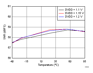
fIN = 1.78 GHz, AIN = –2 dBFS
Figure 6-47 Signal-to-Noise Ratio vs. DVDD Supply and Temperature
GUID-95140B92-E35C-4373-B53E-CBC9A3FD8AF6-low.gif
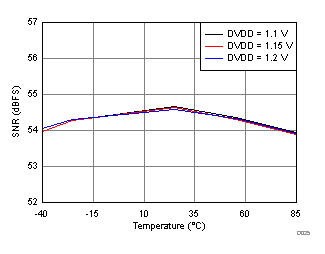
fIN = 3.5 GHz, AIN = –3 dBFS with 2-dB digital gain
Figure 6-49 Signal-to-Noise Ratio vs. DVDD Supply and Temperature
GUID-EE86170C-01DF-4568-88C0-F81FD229309E-low.gif
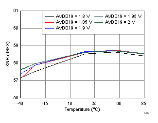
fIN = 1.78 GHz, AIN = –2 dBFS
Figure 6-51 Signal-to-Noise Ratio vs. AVDD19 Supply and Temperature
GUID-B6567B08-B05D-4877-BC35-6B28F71C5EBF-low.gif
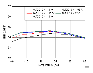
fIN = 3.5 GHz, AIN = –3 dBFS with 2-dB digital gain
Figure 6-53 Signal-to-Noise Ratio vs. AVDD19 Supply and Temperature
GUID-06469AD6-01A6-4FA3-9C1D-1A2F748F1293-low.gif
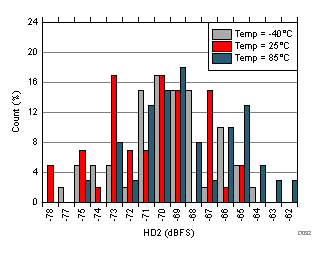
fIN = 1.78 GHz
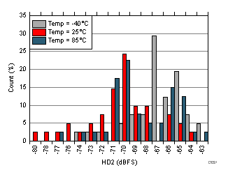
Figure 6-55 HD2 Histogram at AVDD19 = 1.8 V
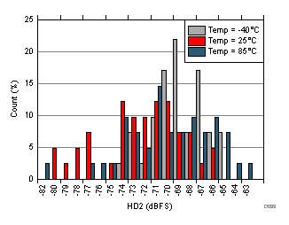
GUID-C497D3A9-9354-42E7-AE43-5908ADCDD3A9-low.gif
fIN = 1.78 GHz
Figure 6-57 HD2 Histogram at AVDD19 = 2.0 V
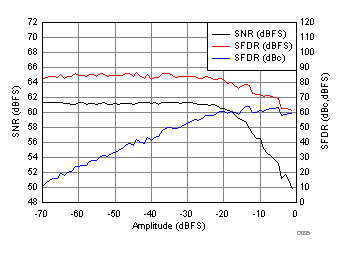
GUID-46A99426-B8E9-4202-877F-6910CBA652F5-low.gif
fIN = 3.5 GHz, AIN = –3 dBFS with 2-dB digital gain
Figure 6-59 Performance vs. Amplitude
GUID-D9BBD5BE-A540-4BED-B5B1-A772D95B5DB6-low.gif
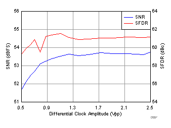
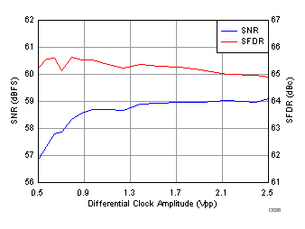
fIN = 3.5 GHz, AIN = –3 dBFS
Figure 6-61 Performance vs. Clock Amplitude
GUID-BDF7DE06-1E52-4F06-9C1B-080B7389741B-low.gif
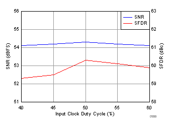
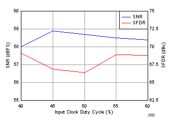
fIN = 3.5 GHz, AIN = –3 dBFS with 2-dB digital gain
Figure 6-63 Performance vs. Clock Duty Cycle
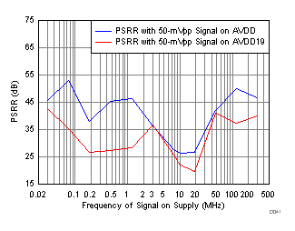
GUID-5DD4C331-4AA0-4180-B754-21A21B720029-low.gifFigure 6-65 Power-Supply Rejection Ratio vs. Tone Frequency
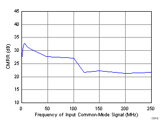
GUID-A7D0448D-CE6F-40CD-9CFB-8A4D95D8A2F3-low.gif
fIN = 1.8 GHz, AOUT = –2 dBFS
Figure 6-67 Common-Mode Rejection Ratio vs. Tone Frequency
GUID-7D60BA19-D3C2-4276-B03A-2EEDEEDE83AC-low.gif
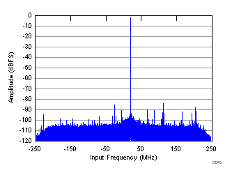
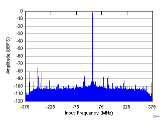
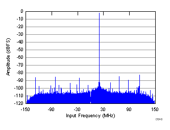
fIN = 1.78 GHz, AIN = –2 dBFS, fS = 2949.12 MSPS, SNR = 61.6 dBFS, SFDR (includes IL) = 82 dBc
Figure 6-69 FFT in 6x Decimation (Complex Output)
GUID-A34EA268-D3F4-441F-A154-B6C81BDCDBE3-low.gif
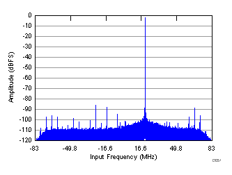
fIN = 1.78 GHz, AIN = –2 dBFS, fS = 2949.12 MSPS, SNR = 63 dBFS, SFDR (includes IL) = 82 dBc
Figure 6-71 FFT in 9x Decimation (Complex Output)
GUID-56A175D2-EFC1-4F9F-8389-88F1FE4D3610-low.gif
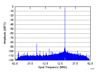
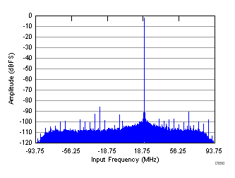
fIN = 1.78 GHz, AIN = –2 dBFS, fS = 2949.12 MSPS, SNR = 63.7 dBFS, SFDR (includes IL) = 83 dBc
Figure 6-73 FFT in 12x Decimation (Complex Output)
GUID-AA55E762-09BA-48EE-84A9-B23FB676F561-low.gif
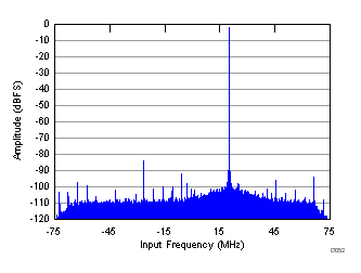
fIN = 1.78 GHz, AIN = –2 dBFS, fS = 2949.12 MSPS, SNR = 64 dBFS, SFDR (includes IL) = 83 dBc
Figure 6-75 FFT in 18x Decimation (Complex Output)
GUID-64D4636A-27F8-4E53-BCB2-F27B86DF9E01-low.gif
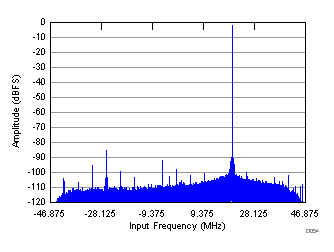
fIN = 1.78 GHz, AIN = –2 dBFS, fS = 2949.12 MSPS, SNR = 64.4 dBFS, SFDR (includes IL) = 82 dBc
Figure 6-77 FFT in 24x Decimation (Complex Output)
GUID-664FC418-79B3-4BB6-901F-B292E27C2D01-low.gif
SNR = 62.4 dBFS; SFDR = 71 dBc; HD2 = –71 dBc; HD3 = –83 dBc; non HD2, HD3 = 82 dBc; IL spur = 80 dBc; fIN = 100 MHz
Figure 6-4 FFT for 100-MHz Input Signal (fS = 2457.6 MSPS)
GUID-4C26BD18-9EF4-475C-84A8-C133F1D24CC4-low.gif
SNR = 62.1 dBFS; SFDR = 76 dBc; HD2 = –76 dBc; HD3 = –83 dBc; non HD2, HD3 = 82 dBc; IL spur = 83 dBc; fIN = 900 MHz
Figure 6-6 FFT for 900-MHz Input Signal (fS = 2457.6 MSPS)
GUID-AF524CA7-5FE6-425D-9AD5-11EF93C0D22E-low.gif
SNR = 58 dBFS; SFDR = 69 dBc; HD2 = –69 dBc; HD3 = –75 dBc; non HD2, HD3 = 74 dBc; IL spur = 78 dBc; fIN = 1.85 GHz
Figure 6-8 FFT for 1850-MHz Input Signal (fS = 2457.6 MSPS)
GUID-27A5975C-4ACD-4A0C-A5D8-B38E01D6414D-low.gif
SNR = 57.5 dBFS; SFDR = 70 dBc; HD2 = –70 dBc; HD3 = –81 dBc; non HD2, HD3 = 75 dBc; IL spur = 77 dBc; fIN = 2.1 GHz
Figure 6-10 FFT for 2100-MHz Input Signal (fS = 2457.6 MSPS)
GUID-03FB2D4D-61E0-4829-8691-8D234E3D6A31-low.gif
SNR = 55.4 dBFS; SFDR = 60 dBc; HD2 = –60 dBc; HD3 = –67 dBc; non HD2, HD3 = 72 dBc; IL spur = 75 dBc; fIN = 2.6 GHz
Figure 6-12 FFT for 2600-MHz Input Signal (fS = 2457.6 MSPS)
GUID-6E4D5CFB-DEDD-4F01-959E-CE3AEFC1267B-low.gif
SNR = 53.6 dBFS; SFDR = 47 dBc; HD2 = –50 dBc; HD3 = –47 dBc; non HD2, HD3 = 70 dBc; IL spur = 67 dBc; fIN = 3.5 GHz, AIN = –3 dBFS with 2-dB gain
Figure 6-14 FFT for 3500-MHz Input Signal (fS = 2457.6 MSPS)
GUID-76DCA644-AFEA-403A-B5F8-7FFCB49B8D9E-low.gif
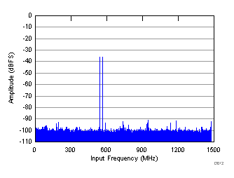
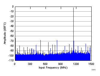
fIN1 = 900 MHz, fIN2 = 950 MHz, AIN = –36 dBFS, IMD = 97 dBFS
Figure 6-16 FFT for Two-Tone Input Signal (–36 dBFS)
GUID-9AEFFE31-FB77-4B35-8690-11E90AAC4A81-low.gif
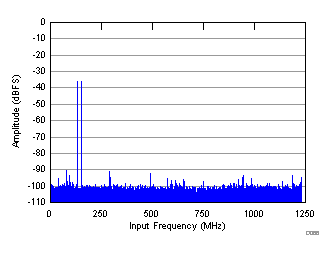
fIN1 = 900 MHz, fIN2 = 950 MHz, AIN = –36 dBFS, IMD = 92 dBFS
Figure 6-18 FFT for Two-Tone Input Signal (–36 dBFS, fS = 2457.6 MSPS)
GUID-0F4C82F0-43E2-4851-83C4-2C3927FE9AA8-low.gif
fIN1 = 1.77 GHz, fIN2 = 1.790 GHz, AIN = –36 dBFS, IMD = 97 dBFS
Figure 6-20 FFT for Two-Tone Input Signal (–36 dBFS)
GUID-5BF892F0-D1E2-47AC-ABF0-028BEBE0916C-low.gif
fIN1 = 1.77 GHz, fIN2 = 1.790 GHz, AIN = –36 dBFS, IMD = 96 dBFS
Figure 6-22 FFT for Two-Tone Input Signal (–36 dBFS, fS = 2457.6 MSPS)
GUID-708F25BB-2058-4D54-9CDD-F8DD94B0DBA1-low.gif
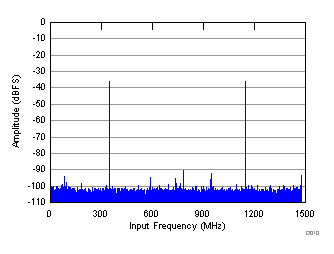
fIN1 = 1.8 GHz, fIN2 = 2.6 GHz, AIN = –36 dBFS, IMD = 94 dBFS
Figure 6-24 FFT for Two-Tone Input Signal
GUID-7BC3E904-7AD8-497F-A45F-DBDB636A2FC6-low.gif
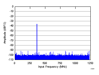
fIN1 = 2.09 MHz, fIN2 = 2.1 GHz, AIN = –36 dBFS, IMD = 94 dBFS
Figure 6-26 FFT for Two-Tone Input Signal (–36 dBFS, fS = 2457.6 MSPS)
GUID-CC806375-4D7C-4AD7-A82F-E23668FF4292-low.gif
fIN1 = 3.49 GHz, fIN2 = 3.51 GHz, IMD = 92 dBFS, AIN = –3 dBFS with 2-dB gain
Figure 6-28 FFT for Two-Tone Input Signal (–36 dBFS)
GUID-7AF534D2-72B7-48CD-80CF-5EAA58AF5A69-low.gif
fIN1 = 2.59 GHz, fIN2 = 2.6 GHz, AIN = –36 dBFS, IMD = 92 dBFS
Figure 6-30 FFT for Two-Tone Input Signal (–36 dBFS, fS = 2457.6 MSPS)
GUID-2D4BC6DD-09FD-4099-B869-D6CC11059CA5-low.gif
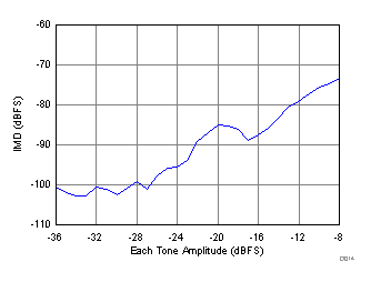
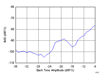
fIN1 = 1.77 GHz, fIN2 = 1.79 GHz
Figure 6-32 Intermodulation Distortion vs. Input Amplitude (1770 MHz and 1790 MHz, fS = 2457.6 MSPS)
GUID-09D82C20-57DA-45F5-BB54-CD88354AA7E5-low.gif
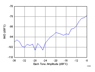
fIN1 = 2.09 GHz, fIN2 = 2.1 GHz
Figure 6-34 Intermodulation Distortion vs. Input Amplitude (1800 MHz and 2600 MHz, fS = 2457.6 MSPS)
GUID-E4021523-CD78-44D5-84ED-E9024676C752-low.gif
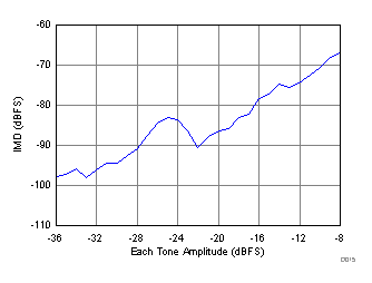
fIN1 = 2.59GHz, fIN2 = 2.6 GHz
Figure 6-36 Intermodulation Distortion vs. Input Amplitude (3490 MHz and 3510 MHz, fS = 2457.6 MSPS)
GUID-AB8E8F71-1C0F-4BE3-9DE1-04D3C68C0D23-low.gif
AOUT = –2 dBFS with 0-dB gain for fIN less than 3 GHz, AOUT = –3 dBFS with 2-dB gain for fIN more than 3 GHz
Figure 6-38 Spurious-Free Dynamic Range vs. Input Frequency (fS = 2457.6 MSPS)
GUID-04EDCA77-308D-4DB1-9CE2-C7BCC2C55199-low.gif
AOUT = –2 dBFS with 0-dB gain for fIN less than 3 GHz, AOUT = –3 dBFS with 2-dB gain for fIN more than 3 GHz
Figure 6-40 IL Spur vs. Input Frequency (fS = 2457.6 MSPS)
GUID-378BCC4E-57BD-4C07-90E0-2C87399AD0E2-low.gif
AOUT = –2 dBFS with 0-dB gain for fIN less than 3 GHz, AOUT = –3 dBFS with 2-dB gain for fIN more than 3 GHz
Figure 6-42 Signal-to-Noise Ratio vs. Input Frequency (fS = 2457.6 MSPS)
GUID-2F214197-31CA-4CB9-9BBD-6109E83ACF8D-low.gif
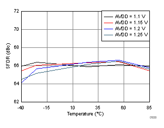
fIN = 1.78 GHz, AIN = –2 dBFS
Figure 6-44 Spurious-Free Dynamic Range vs. AVDD Supply and Temperature
GUID-4EA4198A-D671-40AF-9C27-1BE1EBDCD062-low.gif
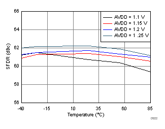
fIN = 3.5GHz, AIN = –3 dBFS with 2-dB digital gain
Figure 6-46 Spurious-Free Dynamic Range vs. AVDD Supply and Temperature
GUID-FCD28E72-AA3B-4E4B-A056-11DC484C1182-low.gif
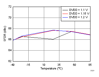
fIN = 1.78 GHz, AIN = –2 dBFS
Figure 6-48 Spurious-Free Dynamic Range vs. DVDD Supply and Temperature
GUID-4505D09F-1F8C-4583-A539-6D12FB36CEDC-low.gif
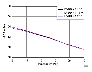
fIN = 3.5 GHz, AIN = –3 dBFS with 2-dB digital gain
Figure 6-50 Spurious-Free Dynamic Range vs. DVDD Supply and Temperature
GUID-BA24D21D-6ED1-4A9B-AAE2-4C02D5647EF7-low.gif
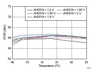
fIN = 1.78 GHz, AIN = –2 dBFS
Figure 6-52 Spurious-Free Dynamic Range vs. AVDD19 Supply and Temperature
GUID-1B9DC9E2-EEF4-41D0-AC9A-9A9EE50A9ACB-low.gif
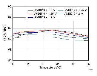
fIN = 3.5 GHz, AIN = –3 dBFS with 2-dB digital gain
Figure 6-54 Spurious-Free Dynamic Range vs. AVDD19 Supply and Temperature
GUID-D3BE0D9D-5853-48DA-8F3A-787699FE3451-low.gif
fIN = 1.78 GHz
Figure 6-56 HD2 Histogram at AVDD19 = 1.9 V
GUID-0750FAAB-ECCD-49B0-A14F-2427FDBE2911-low.gif
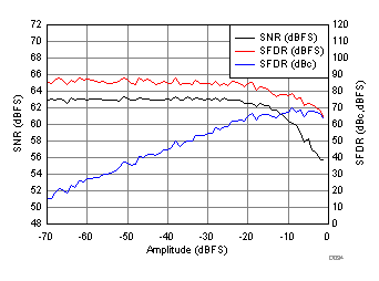
fIN = 1.78 GHz, AIN = –2 dBFS
Figure 6-58 Performance vs. Amplitude
GUID-5DDE81EF-FEAE-40D0-A374-52BCCC4E5572-low.gif
fIN = 1.78 GHz, AIN = –2 dBFS
Figure 6-60 Performance vs. Clock Amplitude
GUID-56E0961A-21C8-41D5-8420-4A0CE659B541-low.gif
fIN = 1.78 GHz, AIN = –2 dBFS
Figure 6-62 Performance vs. Clock Duty Cycle
GUID-B04B5485-16D5-4E20-96A5-EE7C422F6CA4-low.gif
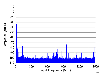
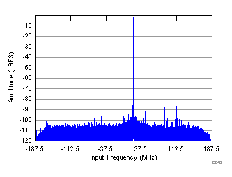
fIN = 3.5 GHz, AIN = –3 dBFS, PSRR = 37 dB, fPSRR = 3 MHz, APSRR = 50 mVPP, AVDD = 1.9 V
Figure 6-64 Power-Supply Rejection Ratio FFT for Test Signal on AVDD Supply
GUID-29E874C2-CB5F-43A4-9D04-5B95C26AA07F-low.gif
CMRR = 32 dB, fCMRR = 32 dB, APSRR = 50 mVPP
Figure 6-66 Common-Mode Rejection Ratio FFT
GUID-9E187F1E-21CE-4058-A973-9EC616B17FAE-low.gif
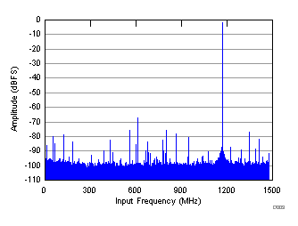
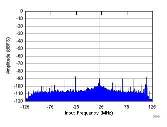
fIN = 1.78 GHz, AIN = –2 dBFS, fS = 2949.12 MSPS, SNR = 60.6 dBFS, SFDR (includes IL) = 75 dBc
Figure 6-68 FFT in 4x Decimation (Complex Output)
GUID-ABBE97CF-15B6-4034-A910-CB14055FE675-low.gif
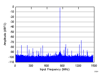
fIN = 1.78 GHz, AIN = –2 dBFS, fS = 2949.12 MSPS, SNR = 62.6 dBFS, SFDR (includes IL) = 86 dBc
Figure 6-70 FFT in 8x Decimation (Complex Output)
GUID-D97B2EFE-8550-4816-B651-B7995C192167-low.gif
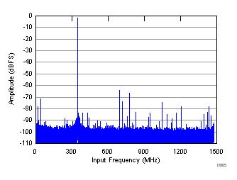
fIN = 1.78 GHz, AIN = –2 dBFS, fS = 2949.12 MSPS, SNR = 63.3 dBFS, SFDR (includes IL) = 81 dBc
Figure 6-72 FFT in 10x Decimation (Complex Output)
GUID-4AA20C53-2B20-4E20-BF3B-FBE9E4D54959-low.gif
fIN = 1.78 GHz, AIN = –2 dBFS, fS = 2949.12 MSPS, SNR = 63.9 dBFS, SFDR (includes IL) = 83 dBc
Figure 6-74 FFT in 16x Decimation (Complex Output)
GUID-7992EEEF-0766-456D-81A0-07E4AF55ED6D-low.gif
fIN = 1.78 GHz, AIN = –2 dBFS, fS = 2949.12 MSPS, SNR = 64.4 dBFS, SFDR (includes IL) = 84 dBc
Figure 6-76 FFT in 20x Decimation (Complex Output)
GUID-9C240314-C56A-485A-A307-F69CCF4D068E-low.gif
fIN = 1.78 GHz, AIN = –2 dBFS, fS = 2949.12 MSPS, SNR = 64.5 dBFS, SFDR (includes IL) = 79 dBc
Figure 6-78 FFT in 32x Decimation (Complex Output)