ZHCSE80B July   2014  – April 2017 ADC3441 , ADC3442 , ADC3443 , ADC3444

PRODUCTION DATA.  

  1. 特性
  2. 应用
  3. 说明
  4. 修订历史记录
  5. Device Comparison Table
  6. Pin Configuration and Functions
  7. Specifications
    1. 7.1  Absolute Maximum Ratings
    2. 7.2  ESD Ratings
    3. 7.3  Recommended Operating Conditions
    4. 7.4  Thermal Information
    5. 7.5  Electrical Characteristics: General
    6. 7.6  Electrical Characteristics: ADC3441, ADC3442
    7. 7.7  Electrical Characteristics: ADC3443, ADC3444
    8. 7.8  AC Performance: ADC3441
    9. 7.9  AC Performance: ADC3442
    10. 7.10 AC Performance: ADC3443
    11. 7.11 AC Performance: ADC3444
    12. 7.12 Digital Characteristics
    13. 7.13 Timing Requirements: General
    14. 7.14 Timing Requirements: LVDS Output
    15. 7.15 Typical Characteristics: ADC3441
    16. 7.16 Typical Characteristics: ADC3442
    17. 7.17 Typical Characteristics: ADC3443
    18. 7.18 Typical Characteristics: ADC3444
    19. 7.19 Typical Characteristics: Common
    20. 7.20 Typical Characteristics: Contour
  8. Parameter Measurement Information
    1. 8.1 Timing Diagrams
  9. Detailed Description
    1. 9.1 Overview
    2. 9.2 Functional Block Diagram
    3. 9.3 Feature Description
      1. 9.3.1 Analog Inputs
      2. 9.3.2 Clock Input
        1. 9.3.2.1 Using the SYSREF Input
        2. 9.3.2.2 SNR and Clock Jitter
      3. 9.3.3 Digital Output Interface
        1. 9.3.3.1 One-Wire Interface: 14x Serialization
        2. 9.3.3.2 Two-Wire Interface: 7x Serialization
    4. 9.4 Device Functional Modes
      1. 9.4.1 Input Clock Divider
      2. 9.4.2 Chopper Functionality
      3. 9.4.3 Power-Down Control
      4. 9.4.4 Internal Dither Algorithm
      5. 9.4.5 Summary of Performance Mode Registers
    5. 9.5 Programming
      1. 9.5.1 Serial Interface
        1. 9.5.1.1 Register Initialization
          1. 9.5.1.1.1 Serial Register Write
          2. 9.5.1.1.2 Serial Register Readout
      2. 9.5.2 ADC3441 Power-Up Requirements
    6. 9.6 Register Maps
      1. 9.6.1 Serial Register Description
        1. 9.6.1.1  Register 01h (address = 01h)
        2. 9.6.1.2  Register 03h (address = 03h)
        3. 9.6.1.3  Register 04h (address = 04h)
        4. 9.6.1.4  Register 05h (address = 05h)
        5. 9.6.1.5  Register 06h (address = 06h)
        6. 9.6.1.6  Register 07h (address = 07h)
        7. 9.6.1.7  Register 09h (address = 09h)
        8. 9.6.1.8  Register 0Ah (address = 0Ah)
        9. 9.6.1.9  Register 0Bh (address = 0Bh)
        10. 9.6.1.10 Register 13h (address = 13h)
        11. 9.6.1.11 Register 0Eh (address = 0Eh)
        12. 9.6.1.12 Register 0Fh (address = 0Fh)
        13. 9.6.1.13 Register 15h (address = 15h)
        14. 9.6.1.14 Register 25h (address = 25h)
        15. 9.6.1.15 Register 27h (address = 27h)
        16. 9.6.1.16 Register 11Dh (address = 11Dh)
        17. 9.6.1.17 Register 122h (address = 122h)
        18. 9.6.1.18 Register 134h (address = 134h)
        19. 9.6.1.19 Register 139h (address = 139h)
        20. 9.6.1.20 Register 21Dh (address = 21Dh)
        21. 9.6.1.21 Register 222h (address = 222h)
        22. 9.6.1.22 Register 234h (address = 234h)
        23. 9.6.1.23 Register 239h (address = 239h)
        24. 9.6.1.24 Register 308h (address = 308h)
        25. 9.6.1.25 Register 41Dh (address = 41Dh)
        26. 9.6.1.26 Register 422h (address = 422h)
        27. 9.6.1.27 Register 434h (address = 434h)
        28. 9.6.1.28 Register 439h (address = 439h)
        29. 9.6.1.29 Register 51Dh (address = 51Dh)
        30. 9.6.1.30 Register 522h (address = 522h)
        31. 9.6.1.31 Register 534h (address = 534h)
        32. 9.6.1.32 Register 539h (address = 539h)
        33. 9.6.1.33 Register 608h (address = 608h)
        34. 9.6.1.34 Register 70Ah (address = 70Ah)
  10. 10Application and Implementation
    1. 10.1 Application Information
    2. 10.2 Typical Applications
      1. 10.2.1 Driving Circuit Design: Low Input Frequencies
        1. 10.2.1.1 Design Requirements
        2. 10.2.1.2 Detailed Design Procedure
        3. 10.2.1.3 Application Curve
      2. 10.2.2 Driving Circuit Design: Input Frequencies Between 100 MHz to 230 MHz
        1. 10.2.2.1 Design Requirements
        2. 10.2.2.2 Detailed Design Procedure
        3. 10.2.2.3 Application Curve
      3. 10.2.3 Driving Circuit Design: Input Frequencies Greater than 230 MHz
        1. 10.2.3.1 Design Requirements
        2. 10.2.3.2 Detailed Design Procedure
        3. 10.2.3.3 Application Curve
  11. 11Power Supply Recommendations
  12. 12Layout
    1. 12.1 Layout Guidelines
    2. 12.2 Layout Example
  13. 13器件和文档支持
    1. 13.1 相关链接
    2. 13.2 接收文档更新通知
    3. 13.3 社区资源
    4. 13.4 商标
    5. 13.5 静电放电警告
    6. 13.6 Glossary
  14. 14机械、封装和可订购信息

封装选项

机械数据 (封装 | 引脚)
散热焊盘机械数据 (封装 | 引脚)
订购信息

Pin Configuration and Functions

RTQ Package
56-Pin VQFN
Top View
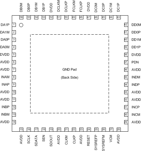
ADC3441 ADC3442 ADC3443 ADC3444 Pin_dgm_SBAS670.gif

Pin Functions

PIN I/O DESCRIPTION
NAME NO.
AVDD 6, 7, 10, 11, 14, 15, 20, 23, 28, 29, 32, 33, 36 I Analog 1.8-V power supply, decoupled with capacitors
CLKM 21 I Negative differential clock input for the ADC
CLKP 22 I Positive differential clock input for the ADC
DA0M 4 O Negative serial LVDS output for wire-0 of channel A
DA0P 3 O Positive serial LVDS output for wire-0 of channel A
DA1M 2 O Negative serial LVDS output for wire-1 of channel A
DA1P 1 O Positive serial LVDS output for wire-1 of channel A
DB0M 56 O Negative serial LVDS output for wire-0 of channel B
DB0P 55 O Positive serial LVDS output for wire-0 of channel B
DB1M 54 O Negative serial LVDS output for wire-1 of channel B
DB1P 53 O Positive serial LVDS output for wire-1 of channel B1
DC0M 46 O Negative serial LVDS output for wire-0 of channel C
DC0P 45 O Positive serial LVDS output for wire-0 of channel C
DC1M 44 O Negative serial LVDS output for wire-1 of channel C
DC1P 43 O Positive serial LVDS output for wire-1 of channel C
DD0M 42 O Negative serial LVDS output for wire-0 of channel D
DD0P 41 O Positive serial LVDS output for wire-0 of channel D
DD1M 40 O Negative serial LVDS output for wire-1 of channel D
DD1P 39 O Positive serial LVDS output for wire-1 of channel D
DCLKM 51 O Negative bit clock output
DCLKP 50 O Positive bit clock output
DVDD 5, 38, 47, 52 I Digital 1.8-V power supply, decoupled with capacitors
FCLKM 49 O Negative frame clock output
FCLKP 48 O Positive frame clock output
GND PowerPAD™ I Ground, 0 V. Connect to the printed circuit board (PCB) ground plane.
INAM 8 I Negative differential analog input for channel A
INAP 9 I Positive differential analog input for channel A
INBM 13 I Negative differential analog input for channel B
INBP 12 I Positive differential analog input for channel B
INCM 30 I Negative differential analog input for channel C
INCP 31 I Positive differential analog input for channel C
INDM 35 I Negative differential analog input for channel D
INDP 34 I Positive differential analog input for channel D
PDN 37 I Power-down control; active high. This pin may be configured through the SPI.
This pin has an internal 150-kΩ pulldown resistor.
RESET 24 I Hardware reset; active high. This pin has an internal 150-kΩ pulldown resistor.
SCLK 16 I Serial interface clock input. This pin has an internal 150-kΩ pulldown resistor.
SDATA 17 I Serial interface data input. This pin has an internal 150-kΩ pulldown resistor.
SDOUT 19 O Serial interface data output
SEN 18 I Serial interface enable; active low.
This pin has an internal 150-kΩ pullup resistor to AVDD.
SYSREFM 26 I Negative external SYSREF input
SYSREFP 25 I Positive external SYSREF input
VCM 27 O Common-mode voltage for analog inputs