ZHCSLJ1C July 2020 – December 2022 ADC3541 , ADC3542 , ADC3543
PRODUCTION DATA
- 1 特性
- 2 应用
- 3 说明
- 4 Revision History
- 5 Pin Configuration and Functions
-
6 Specifications
- 6.1 Absolute Maximum Ratings
- 6.2 ESD Ratings
- 6.3 Recommended Operating Conditions
- 6.4 Thermal Information
- 6.5 Electrical Characteristics - Power Consumption
- 6.6 Electrical Characteristics - DC Specifications
- 6.7 Electrical Characteristics - AC Specifications ADC3541
- 6.8 Electrical Characteristics - AC Specifications ADC3542
- 6.9 Electrical Characteristics - AC Specifications ADC3543
- 6.10 Timing Requirements
- 6.11 Typical Characteristics: ADC3541
- 6.12 Typical Characteristics: ADC3542
- 6.13 Typical Characteristics: ADC3543
- 7 Parameter Measurement Information
- 8 Detailed Description
- 9 Application Information Disclaimer
- 10Power Supply Recommendations
- 11Layout
- 12Device and Documentation Support
- 13Mechanical, Packaging, and Orderable Information
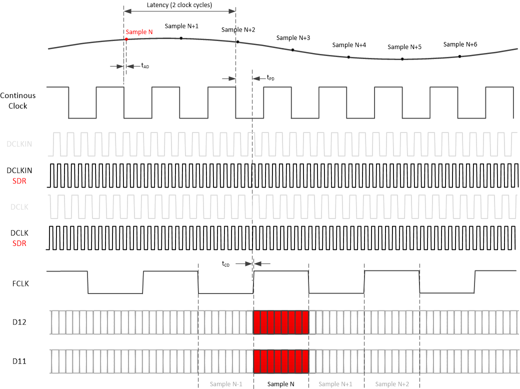
8.3.5.2.1 SDR Output Clocking
The ADC354x provides a SDR output clocking option for all serial CMOS output modes (including decimation) which is enabled using the SPI interface. In serial CMOS mode by default the data is output on rising and falling edge of DCLK. In SDR clocking mode, DCLKIN has to be twice as fast as the default DCLKIN so that the output data are clocked out only on DCLK rising edge.
Internally DCLKIN is divided by 2 for data processing and this operation can add 1 extra clock cycle latency to the ADC latency.
 Figure 8-40 SDR Output Clocking