ZHCSLJ1C July 2020 – December 2022 ADC3541 , ADC3542 , ADC3543
PRODUCTION DATA
- 1 特性
- 2 应用
- 3 说明
- 4 Revision History
- 5 Pin Configuration and Functions
-
6 Specifications
- 6.1 Absolute Maximum Ratings
- 6.2 ESD Ratings
- 6.3 Recommended Operating Conditions
- 6.4 Thermal Information
- 6.5 Electrical Characteristics - Power Consumption
- 6.6 Electrical Characteristics - DC Specifications
- 6.7 Electrical Characteristics - AC Specifications ADC3541
- 6.8 Electrical Characteristics - AC Specifications ADC3542
- 6.9 Electrical Characteristics - AC Specifications ADC3543
- 6.10 Timing Requirements
- 6.11 Typical Characteristics: ADC3541
- 6.12 Typical Characteristics: ADC3542
- 6.13 Typical Characteristics: ADC3543
- 7 Parameter Measurement Information
- 8 Detailed Description
- 9 Application Information Disclaimer
- 10Power Supply Recommendations
- 11Layout
- 12Device and Documentation Support
- 13Mechanical, Packaging, and Orderable Information
10 Power Supply Recommendations
The ADC354x requires two different power-supplies. The AVDD rail provides power for the internal analog circuits and the ADC itself while the IOVDD rail powers the digital interface and the internal digital circuits like decimation filter or output interface mapper. Power sequencing is not required.
The AVDD power supply must be low noise in order to achieve data sheet performance. In applications operating near DC, the 1/f noise contribution of the power supply needs to be considered as well. The ADC is designed for very good PSRR which aides with the power supply filter design.
There are two recommended power-supply architectures:
- Step down using high-efficiency switching converters, followed by a second stage of regulation using a low noise LDO to provide switching noise reduction and improved voltage accuracy.
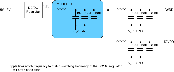
- Directly step down the final ADC supply voltage using high-efficiency switching converters. This approach provides the best efficiency, but care must be taken to ensure switching noise is minimized to prevent degraded ADC performance.
TI WEBENCH® Power Designer can be used to select and design the individual power-supply elements needed: see the WEBENCH® Power Designer
Recommended switching regulators for the first stage include the TPS62821, and similar devices.
Recommended low dropout (LDO) linear regulators include the TPS7A4701, TPS7A90, LP5901, and similar devices.
For the switch regulator only approach, the ripple filter must be designed with a notch frequency that aligns with the switching ripple frequency of the DC/DC converter. Note the switching frequency reported from WEBENCH® and design the EMI filter and capacitor combination to have the notch frequency centered as needed. Figure 10-2 and Figure 10-3 illustrate the two approaches.
AVDD and IOVDD supply voltages should not be shared in order to prevent digital switching noise from coupling into the analog signal chain.
 Figure 10-2 Example: LDO Linear Regulator
Approach
 Figure 10-3 Example Switcher-Only
Approach