ZHCSRD5 December   2022 ADC3544

PRODUCTION DATA  

  1. 特性
  2. 应用
  3. 说明
  4. Revision History
  5. Pin Configuration and Functions
  6. Specifications
    1. 6.1 Absolute Maximum Ratings
    2. 6.2 ESD Ratings
    3. 6.3 Recommended Operating Conditions
    4. 6.4 Thermal Information
    5. 6.5 Electrical Characteristics - Power Consumption
    6. 6.6 Electrical Characteristics - DC Specifications
    7. 6.7 Electrical Characteristics - AC Specifications
    8. 6.8 Timing Requirements
    9. 6.9 Typical Characteristics
  7. Parameter Measurement Information
  8. Detailed Description
    1. 8.1 Overview
    2. 8.2 Functional Block Diagram
    3. 8.3 Feature Description
      1. 8.3.1 Analog Input
        1. 8.3.1.1 Analog Input Bandwidth
        2. 8.3.1.2 Analog Front End Design
          1. 8.3.1.2.1 Sampling Glitch Filter Design
          2. 8.3.1.2.2 Single Ended Input
          3. 8.3.1.2.3 Analog Input Termination and DC Bias
            1. 8.3.1.2.3.1 AC-Coupling
            2. 8.3.1.2.3.2 DC-Coupling
      2. 8.3.2 Clock Input
        1. 8.3.2.1 Single Ended vs Differential Clock Input
      3. 8.3.3 Voltage Reference
        1. 8.3.3.1 Internal voltage reference
        2. 8.3.3.2 External voltage reference (VREF)
        3. 8.3.3.3 External voltage reference with internal buffer (REFBUF)
      4. 8.3.4 Digital Down Converter
        1. 8.3.4.1 Digital Filter Operation
        2. 8.3.4.2 FS/4 Mixing with Real Output
        3. 8.3.4.3 Numerically Controlled Oscillator (NCO) and Digital Mixer
        4. 8.3.4.4 Decimation Filter
        5. 8.3.4.5 SYNC
        6. 8.3.4.6 Output Formatting with Decimation
          1. 8.3.4.6.1 Parallel CMOS
          2. 8.3.4.6.2 Serialized CMOS Interface
      5. 8.3.5 Digital Interface
        1. 8.3.5.1 Parallel CMOS Output
        2. 8.3.5.2 Serialized CMOS output
          1. 8.3.5.2.1 SDR Output Clocking
        3. 8.3.5.3 Output Data Format
        4. 8.3.5.4 Output Formatter
        5. 8.3.5.5 Output Bit Mapper
        6. 8.3.5.6 Output Interface/Mode Configuration
          1. 8.3.5.6.1 Configuration Example
      6. 8.3.6 Test Pattern
    4. 8.4 Device Functional Modes
      1. 8.4.1 Normal operation
      2. 8.4.2 Power Down Options
    5. 8.5 Programming
      1. 8.5.1 Configuration using PINs only
      2. 8.5.2 Configuration using the SPI interface
        1. 8.5.2.1 Register Write
        2. 8.5.2.2 Register Read
    6. 8.6 Register Maps
      1. 8.6.1 Detailed Register Description
  9. Application Information Disclaimer
    1. 9.1 Application Information
    2. 9.2 Typical Application
      1. 9.2.1 Design Requirements
      2. 9.2.2 Detailed Design Procedure
        1. 9.2.2.1 Input Signal Path
        2. 9.2.2.2 Sampling Clock
        3. 9.2.2.3 Voltage Reference
      3. 9.2.3 Application Curves
    3. 9.3 Initialization Set Up
      1. 9.3.1 Register Initialization During Operation
    4. 9.4 Power Supply Recommendations
    5. 9.5 Layout
      1. 9.5.1 Layout Guidelines
      2. 9.5.2 Layout Example
  10. 10Device and Documentation Support
    1. 10.1 Receiving Notification of Documentation Updates
    2. 10.2 Trademarks
    3. 10.3 Electrostatic Discharge Caution
    4. 10.4 术语表
  11. 11Mechanical, Packaging, and Orderable Information

封装选项

机械数据 (封装 | 引脚)
散热焊盘机械数据 (封装 | 引脚)
订购信息

Voltage Reference

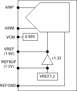
The ADC3544 provides three different options for supplying the voltage reference to the ADC. An external 1.6 V reference can be directly connected to the VREF input; a voltage 1.2 V reference can be connected to the REFBUF input using the internal gain buffer or the internal 1.2V reference can be enabled to generate a 1.6 V reference voltage. For best performance, the reference noise should be filtered by connecting a 10 uF and a 0.1 uF ceramic bypass capacitor to the VREF pin. The internal reference circuitry of the ADC3544 is shown in Figure 8-10.

Note: The voltage reference mode can be selected by using the REFBUF pin as a control pin (Section 8.5.1). If the REFBUF pin is not used for configuration, the REFBUF pin should be connected to AVDD (even though the REFBUF pin has a weak internal pullup to AVDD) and the voltage reference option has to be selected using the SPI interface.
GUID-3BBD0092-F160-4A62-8035-185D97DF0B9F-low.gifFigure 8-10 Different voltage reference options for ADC3544