ZHCSNB7A February   2021  – October 2022 ADC3581 , ADC3582 , ADC3583

PRODUCTION DATA  

  1. 特性
  2. 应用
  3. 说明
  4. Revision History
  5. Pin Configuration and Functions
  6. Specifications
    1. 6.1  Absolute Maximum Ratings
    2. 6.2  ESD Ratings
    3. 6.3  Recommended Operating Conditions
    4. 6.4  Thermal Information
    5. 6.5  Electrical Characteristics - Power Consumption
    6. 6.6  Electrical Characteristics - DC Specifications
    7. 6.7  Electrical Characteristics - AC Specifications
    8. 6.8  Timing Requirements
    9. 6.9  Typical Characteristics - ADC3581
    10. 6.10 Typical Characteristics - ADC3582
    11. 6.11 Typical Characteristics - ADC3583
  7. Parameter Measurement Information
  8. Detailed Description
    1. 8.1 Overview
    2. 8.2 Functional Block Diagram
    3. 8.3 Feature Description
      1. 8.3.1 Analog Input
        1. 8.3.1.1 Analog Input Bandwidth
        2. 8.3.1.2 Analog Front End Design
          1. 8.3.1.2.1 Sampling Glitch Filter Design
          2. 8.3.1.2.2 Analog Input Termination and DC Bias
            1. 8.3.1.2.2.1 AC-Coupling
            2. 8.3.1.2.2.2 DC-Coupling
        3. 8.3.1.3 Auto-Zero Feature
      2. 8.3.2 Clock Input
        1. 8.3.2.1 Single Ended vs Differential Clock Input
        2. 8.3.2.2 Signal Acquisition Time Adjust
      3. 8.3.3 Voltage Reference
        1. 8.3.3.1 Internal voltage reference
        2. 8.3.3.2 External voltage reference (VREF)
        3. 8.3.3.3 External voltage reference with internal buffer (REFBUF)
      4. 8.3.4 Digital Down Converter
        1. 8.3.4.1 DDC MUX for Dual Band Decimation
        2. 8.3.4.2 Digital Filter Operation
        3. 8.3.4.3 FS/4 Mixing with Real Output
        4. 8.3.4.4 Numerically Controlled Oscillator (NCO) and Digital Mixer
        5. 8.3.4.5 Decimation Filter
        6. 8.3.4.6 SYNC
        7. 8.3.4.7 Output Formatting with Decimation
      5. 8.3.5 Digital Interface
        1. 8.3.5.1 Output Formatter
        2. 8.3.5.2 Output Scrambler
        3. 8.3.5.3 Output Bit Mapper
        4. 8.3.5.4 Output Interface/Mode Configuration
          1. 8.3.5.4.1 Configuration Example
        5. 8.3.5.5 Output Data Format
      6. 8.3.6 Test Pattern
    4. 8.4 Device Functional Modes
      1. 8.4.1 Normal Operation
      2. 8.4.2 Power Down Options
    5. 8.5 Programming
      1. 8.5.1 Configuration using PINs only
      2. 8.5.2 Configuration using the SPI interface
        1. 8.5.2.1 Register Write
        2. 8.5.2.2 Register Read
    6. 8.6 Register Map
      1. 8.6.1 Detailed Register Description
  9. Application Information Disclaimer
    1. 9.1 Typical Application
      1. 9.1.1 Design Requirements
      2. 9.1.2 Detailed Design Procedure
        1. 9.1.2.1 Input Signal Path
        2. 9.1.2.2 Sampling Clock
        3. 9.1.2.3 Voltage Reference
      3. 9.1.3 Application Curves
    2. 9.2 Initialization Set Up
      1. 9.2.1 Register Initialization During Operation
    3. 9.3 Power Supply Recommendations
    4. 9.4 Layout
      1. 9.4.1 Layout Guidelines
      2. 9.4.2 Layout Example
  10. 10Device and Documentation Support
    1. 10.1 接收文档更新通知
    2. 10.2 支持资源
    3. 10.3 Trademarks
    4. 10.4 Electrostatic Discharge Caution
    5. 10.5 术语表
  11. 11Mechanical, Packaging, and Orderable Information

封装选项

机械数据 (封装 | 引脚)
散热焊盘机械数据 (封装 | 引脚)
订购信息
DC-Coupling

In DC coupled applications the DC bias needs to be provided from the fully differential amplifier (FDA) using VCM output of the ADC as shown in Figure 8-7. The glitch filter in this case is located between the anti-alias filter and the ADC. No termination may be needed if amplifier is located close to the ADC or if the termination is part of the anti-alias filter.
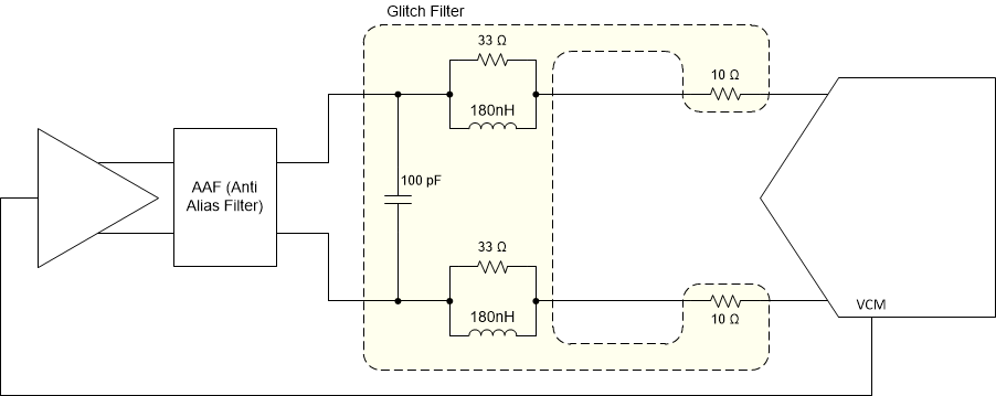
GUID-4FC6183E-B9A5-4840-92B0-9E9D2B844A9C-low.gif Figure 8-7 DC-Coupling: DC bias provided by FDA (glitch filter example for DC - 30 MHz)