ZHCSMB7A October 2020 – May 2022 ADC3641 , ADC3642 , ADC3643
PRODUCTION DATA
- 1 特性
- 2 应用
- 3 说明
- 4 Revision History
- 5 Pin Configuration and Functions
-
6 Specifications
- 6.1 Absolute Maximum Ratings
- 6.2 ESD Ratings
- 6.3 Recommended Operating Conditions
- 6.4 Thermal Information
- 6.5 Electrical Characteristics - Power Consumption
- 6.6 Electrical Characteristics - DC Specifications
- 6.7 Electrical Characteristics - AC Specifications ADC3641
- 6.8 Electrical Characteristics - AC Specifications ADC3642
- 6.9 Electrical Characteristics - AC Specifications ADC3643
- 6.10 Timing Requirements
- 6.11 Typical Characteristics - ADC3641
- 6.12 Typical Characteristics - ADC3642
- 6.13 Typical Characteristics - ADC3643
- 7 Parameter Measurement Information
- 8 Detailed Description
- 9 Application and Implementation
- 10Device and Documentation Support
- 11Mechanical, Packaging, and Orderable Information
8.3.4.6.2 Serialized CMOS
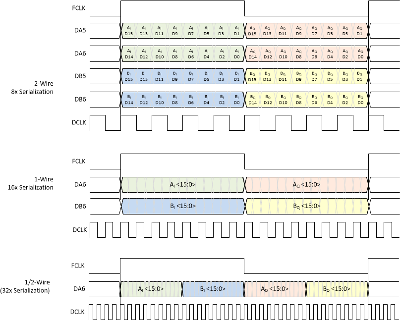
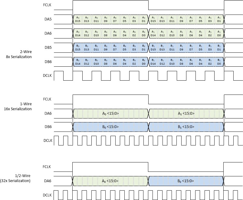
In serialized CMOS mode, the ADC364x device supports complex decimation output Figure 8-38 and real decimation output Figure 8-39. The examples are shown for 16-bit output for 2-wire (8x serialization) and 1-wire (16x serialization).
 Figure 8-38 Output Data Format in Complex Decimation
Table 8-5 illustrates the output interface data rate along with the corresponding DCLK/DCLKIN and FCLK frequencies based on output resolution (R), number of serial CMOS lanes (L) and complex decimation setting (N).
Furthermore the table shows an actual lane rate example for the 2-, 1- and 1/2-wire interface, 16-bit output resolution and complex decimation by 16.
| DECIMATION SETTING | ADC SAMPLING RATE | OUTPUT RESOLUTION | # of WIRES | FCLK | DCLKIN, DCLK | DOUT |
|---|---|---|---|---|---|---|
| N | FS | R | L | FS / N | [DOUT] / 2 | FS x 2 x R / L / N |
| 16 | 65 MSPS | 16 | 2 | 4.0625 MHz | 32.5 MHz | 65 MHz |
| 1 | 65 MHz | 130 MHz | ||||
| 62.5 MSPS | 1/2 | 3.90625 MHz | 125 MHz | 250 MHz |
 Figure 8-39 Output Data Format in Real Decimation
Table 8-6 illustrates the output interface data rate along with the corresponding DCLK/DCLKIN and FCLK frequencies based on output resolution (R), number of serial CMOS lanes (L) and real decimation setting (M).
Furthermore the table shows an actual lane rate example for the 2-, 1- and 1/2-wire interface, 16-bit output resolution and real decimation by 16.
| DECIMATION SETTING | ADC SAMPLING RATE | OUTPUT RESOLUTION | # of WIRES | FCLK | DCLKIN, DCLK | DOUT |
|---|---|---|---|---|---|---|
| M | FS | R | L | FS / M / 2 (L = 2) FS / M (L = 1, 1/2) | [DOUT] / 2 | FS x R / L / M |
| 16 | 65 MSPS | 16 | 2 | 2.03125 MHz | 16.25 MHz | 32.5 MHz |
| 1 | 4.0625 MHz | 32.5 MHz | 65 MHz | |||
| 1/2 | 65 MHz | 130 MHz |