ZHCSQN6 May   2022 ADC3644

PRODUCTION DATA  

  1. 特性
  2. 应用
  3. 说明
  4. Revision History
  5. Pin Configuration and Functions
  6. Specifications
    1. 6.1 Absolute Maximum Ratings
    2. 6.2 ESD Ratings
    3. 6.3 Recommended Operating Conditions
    4. 6.4 Thermal Information
    5. 6.5 Electrical Characteristics - Power Consumption
    6. 6.6 Electrical Characteristics - DC Specifications
    7. 6.7 Electrical Characteristics - AC Specifications
    8. 6.8 Timing Requirements
    9. 6.9 Typical Characteristics
  7. Parameter Measurement Information
  8. Detailed Description
    1. 8.1 Overview
    2. 8.2 Functional Block Diagram
    3. 8.3 Feature Description
      1. 8.3.1 Analog Input
        1. 8.3.1.1 Analog Input Bandwidth
        2. 8.3.1.2 Analog Front End Design
          1. 8.3.1.2.1 Sampling Glitch Filter Design
          2. 8.3.1.2.2 Single Ended Input
          3. 8.3.1.2.3 Analog Input Termination and DC Bias
            1. 8.3.1.2.3.1 AC-Coupling
            2. 8.3.1.2.3.2 DC-Coupling
      2. 8.3.2 Clock Input
        1. 8.3.2.1 Clock Amplitude
        2. 8.3.2.2 Single Ended vs Differential Clock Input
      3. 8.3.3 Voltage Reference
        1. 8.3.3.1 Internal voltage reference
        2. 8.3.3.2 External voltage reference (VREF)
        3. 8.3.3.3 External voltage reference with internal buffer (REFBUF)
      4. 8.3.4 Digital Down Converter
        1. 8.3.4.1 DDC MUX
        2. 8.3.4.2 Digital Filter Operation
        3. 8.3.4.3 FS/4 Mixing with Real Output
        4. 8.3.4.4 Numerically Controlled Oscillator (NCO) and Digital Mixer
        5. 8.3.4.5 Decimation Filter
        6. 8.3.4.6 SYNC
        7. 8.3.4.7 Output Formatting with Decimation
          1. 8.3.4.7.1 Parallel CMOS
          2. 8.3.4.7.2 Serialized CMOS Interface
      5. 8.3.5 Digital Interface
        1. 8.3.5.1 Parallel CMOS Output
        2. 8.3.5.2 Serialized CMOS output
          1. 8.3.5.2.1 SDR Output Clocking
        3. 8.3.5.3 Output Data Format
        4. 8.3.5.4 Output Formatter
        5. 8.3.5.5 Output Bit Mapper
        6. 8.3.5.6 Output Interface or Mode Configuration
          1. 8.3.5.6.1 Configuration Example
      6. 8.3.6 Test Pattern
    4. 8.4 Device Functional Modes
      1. 8.4.1 Normal operation
      2. 8.4.2 Power Down Options
    5. 8.5 Programming
      1. 8.5.1 Configuration using PINs only
      2. 8.5.2 Configuration using the SPI interface
        1. 8.5.2.1 Register Write
        2. 8.5.2.2 Register Read
    6. 8.6 Register Maps
      1. 8.6.1 Detailed Register Description
  9. Application Information Disclaimer
    1. 9.1 Typical Application
      1. 9.1.1 Design Requirements
      2. 9.1.2 Detailed Design Procedure
        1. 9.1.2.1 Input Signal Path
        2. 9.1.2.2 Sampling Clock
        3. 9.1.2.3 Voltage Reference
      3. 9.1.3 Application Curves
    2. 9.2 Initialization Set Up
      1. 9.2.1 Register Initialization During Operation
    3. 9.3 Power Supply Recommendations
    4. 9.4 Layout
      1. 9.4.1 Layout Guidelines
      2. 9.4.2 Layout Example
  10. 10Device and Documentation Support
    1. 10.1 Device Support (Optional)
      1. 10.1.1 Development Support (Optional)
      2. 10.1.2 Device Nomenclature (Optional)
    2. 10.2 Documentation Support (if applicable)
      1. 10.2.1 Related Documentation
    3. 10.3 接收文档更新通知
    4. 10.4 支持资源
    5. 10.5 Trademarks
    6. 10.6 Electrostatic Discharge Caution
    7. 10.7 术语表
  11. 11Mechanical, Packaging, and Orderable Information

封装选项

机械数据 (封装 | 引脚)
散热焊盘机械数据 (封装 | 引脚)
订购信息

Initialization Set Up

After power-up, the internal registers must be initialized to the default values through a hardware reset by applying a high pulse on the RESET pin, as shown in Figure 9-5.

  1. Apply AVDD and IOVDD (no specific sequence required). After AVDD is applied the internal bandgap reference will power up and settle out in ~ 2ms.
  2. Configure REFBUF pin (pull high or low even if configured via SPI later on) and apply the sampling clock.
  3. Apply hardware reset. After hardware reset is released, the default registers are loaded from internal fuses and the internal power up capacitor calibration is initiated. The calibration takes approximately 200000 clock cycles.
  4. Begin programming using SPI interface.
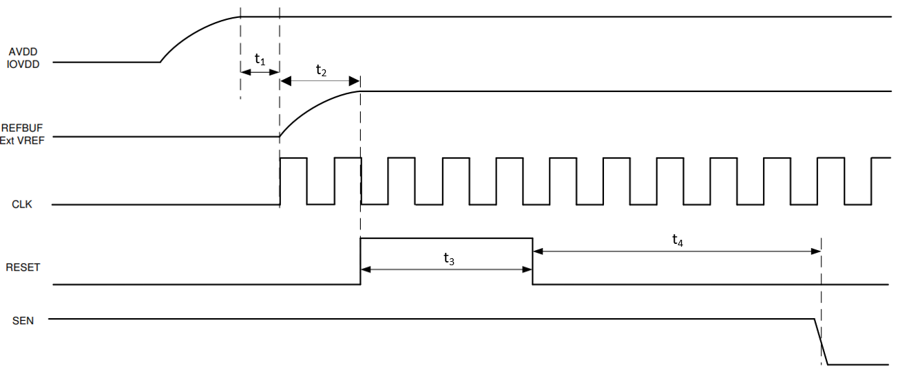
GUID-20211216-SS0I-QSTP-HX9J-NBJTC2VZNCLD-low.pngFigure 9-5 Initialization of serial registers after power up
Table 9-5 Power-up timing
MINTYPMAXUNIT
t1Power-on delay: delay from power up to logic level of REFBUF pin2ms
t2Delay from REFBUF pin logic level to RESET rising edge100ns
t3RESET pulse width1us
t4Delay from RESET disable to SEN active~ 200000clock cycles