ZHCSM31B September   2020  – March 2022 ADC3660

PRODUCTION DATA  

  1. 特性
  2. 应用
  3. 说明
  4. Revision History
  5. Pin Configuration and Functions
  6. Specifications
    1. 6.1 Absolute Maximum Ratings
    2. 6.2 ESD Ratings
    3. 6.3 Recommended Operating Conditions
    4. 6.4 Thermal Information
    5. 6.5 Electrical Characteristics - Power Consumption
    6. 6.6 Electrical Characteristics - DC Specifications
    7. 6.7 Electrical Characteristics - AC Specifications
    8. 6.8 Timing Requirements
    9. 6.9 Typical Characteristics
  7. Parameter Measurement Information
  8. Detailed Description
    1. 8.1 Overview
    2. 8.2 Functional Block Diagram
    3. 8.3 Feature Description
      1. 8.3.1 Analog Input
        1. 8.3.1.1 Analog Input Bandwidth
        2. 8.3.1.2 Analog Front End Design
          1. 8.3.1.2.1 Sampling Glitch Filter Design
          2. 8.3.1.2.2 Analog Input Termination and DC Bias
            1. 8.3.1.2.2.1 AC-Coupling
            2. 8.3.1.2.2.2 DC-Coupling
        3. 8.3.1.3 Auto-Zero Feature
      2. 8.3.2 Clock Input
        1. 8.3.2.1 Single Ended vs Differential Clock Input
        2. 8.3.2.2 Signal Acquisition Time Adjust
      3. 8.3.3 Voltage Reference
        1. 8.3.3.1 Internal voltage reference
        2. 8.3.3.2 External voltage reference (VREF)
        3. 8.3.3.3 External voltage reference with internal buffer (REFBUF)
      4. 8.3.4 Digital Down Converter
        1. 8.3.4.1 DDC MUX
        2. 8.3.4.2 Digital Filter Operation
          1. 8.3.4.2.1 FS/4 Mixing with Real Output
        3. 8.3.4.3 Numerically Controlled Oscillator (NCO) and Digital Mixer
        4. 8.3.4.4 Decimation Filter
        5. 8.3.4.5 SYNC
        6. 8.3.4.6 Output Formatting with Decimation
      5. 8.3.5 Digital Interface
        1. 8.3.5.1 SDR Output Clocking
        2. 8.3.5.2 Output Data Format
        3. 8.3.5.3 Output Formatter
        4. 8.3.5.4 Output Bit Mapper
        5. 8.3.5.5 Output Interface/Mode Configuration
          1. 8.3.5.5.1 Configuration Example
      6. 8.3.6 Test Pattern
    4. 8.4 Device Functional Modes
      1. 8.4.1 Normal Operation
      2. 8.4.2 Power Down Options
      3. 8.4.3 Digital Channel Averaging
    5. 8.5 Programming
      1. 8.5.1 Configuration using PINs only
      2. 8.5.2 Configuration using the SPI interface
        1. 8.5.2.1 Register Write
        2. 8.5.2.2 Register Read
    6. 8.6 Register Maps
      1. 8.6.1 Detailed Register Description
  9. Application and Implementation
    1. 9.1 Typical Application
      1. 9.1.1 Design Requirements
      2. 9.1.2 Detailed Design Procedure
        1. 9.1.2.1 Input Signal Path
        2. 9.1.2.2 Sampling Clock
        3. 9.1.2.3 Voltage Reference
      3. 9.1.3 Application Curves
    2. 9.2 Initialization Set Up
      1. 9.2.1 Register Initialization During Operation
  10. 10Power Supply Recommendations
  11. 11Layout
    1. 11.1 Layout Guidelines
    2. 11.2 Layout Example
  12. 12Device and Documentation Support
    1. 12.1 支持资源
    2. 12.2 Trademarks
    3. 12.3 Electrostatic Discharge Caution
    4. 12.4 术语表
  13. 13Mechanical, Packaging, and Orderable Information

封装选项

机械数据 (封装 | 引脚)
散热焊盘机械数据 (封装 | 引脚)
订购信息

Application Curves

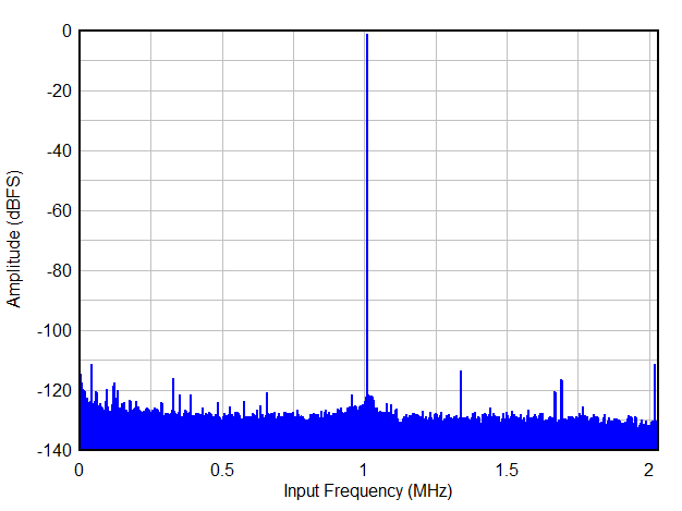
The following FFT plots show the performance of THS4541 driving the ADC3660 operated at 65 MSPS with a full-scale input at -1 dBFS. The first FFT spectrum below shows the performance with a single tone input at FIN = 1 MHz and decimation by 16 (real).

The second FFT spectrum shows the a single tone input at FIN = 5 MHz and complex decimation by 16 where the NCO is programmed to 4.5 MHz.
GUID-20200911-CA0I-PQMP-Q7HK-PXJ5S10P6GND-low.gif

Decimation by 16, real

Figure 9-2 Single Tone FFT at FIN = 1 MHz
GUID-20200911-CA0I-CTHT-W8DD-9M5SSXZH061L-low.gif

Decimation by 16, complex, NCO = 4.5 MHz

Figure 9-3 Single Tone FFT at FIN = 5 MHz