ZHCSHA6E May 2009 – January 2018 ADS1013 , ADS1014 , ADS1015
PRODUCTION DATA.
- 1 特性
- 2 应用
- 3 说明
- 4 Revision History
- 5 Device Comparison Table
- 6 Pin Configuration and Functions
- 7 Specifications
-
8 Detailed Description
- 8.1 Overview
- 8.2 Functional Block Diagrams
- 8.3 Feature Description
- 8.4 Device Functional Modes
- 8.5 Programming
- 8.6 Register Map
-
9 Application and Implementation
- 9.1 Application Information
- 9.2
Typical Application
- 9.2.1 Design Requirements
- 9.2.2
Detailed Design Procedure
- 9.2.2.1 Shunt Resistor Considerations
- 9.2.2.2 Operational Amplifier Considerations
- 9.2.2.3 ADC Input Common-Mode Considerations
- 9.2.2.4 Resistor (R1, R2, R3, R4) Considerations
- 9.2.2.5 Noise and Input Impedance Considerations
- 9.2.2.6 First-order RC Filter Considerations
- 9.2.2.7 Circuit Implementation
- 9.2.2.8 Results Summary
- 9.2.3 Application Curves
- 10Power Supply Recommendations
- 11Layout
- 12器件和文档支持
- 13机械、封装和可订购信息
9.1.7 Quickstart Guide
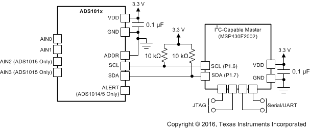
This section provides a brief example of ADS101x communications. See subsequent sections of this data sheet for more detailed explanations. Hardware for this design includes: one ADS101x configured with an I2C address of 1001000; a microcontroller with an I2C interface; discrete components such as resistors, capacitors, and serial connectors; and a 2 V to 5 V power supply. Figure 28 shows the basic hardware configuration.
The ADS101x communicate with the master (microcontroller) through an I2C interface. The master provides a clock signal on the SCL pin and data are transferred using the SDA pin. The ADS101x never drive the SCL pin. For information on programming and debugging the microcontroller being used, see the device-specific product data sheet.
The first byte sent by the master is the ADS101x address, followed by the R/W bit that instructs the ADS101x to listen for a subsequent byte. The second byte is the Address Pointer register byte. The third and fourth bytes sent from the master are written to the register indicated in register address pointer bits P[1:0]. See Figure 15 and Figure 16 for read and write operation timing diagrams, respectively. All read and write transactions with the ADS101x must be preceded by a START condition, and followed by a STOP condition.
For example, to write to the configuration register to set the ADS101x to continuous-conversion mode and then read the conversion result, send the following bytes in this order:
- Write to Config register:
- First byte: 0b10010000 (first 7-bit I2C address followed by a low R/W bit)
- Second byte: 0b00000001 (points to Config register)
- Third byte: 0b10000100 (MSB of the Config register to be written)
- Fourth byte: 0b10000011 (LSB of the Config register to be written)
- Write to Address Pointer register:
- First byte: 0b10010000 (first 7-bit I2C address followed by a low R/W bit)
- Second byte: 0b00000000 (points to Conversion register)
- Read Conversion register:
- First byte: 0b10010001 (first 7-bit I2C address followed by a high R/W bit)
- Second byte: the ADS101x response with the MSB of the Conversion register
- Third byte: the ADS101x response with the LSB of the Conversion register
