ZHCSEB2A October   2015  – November 2015 ADS1018-Q1

PRODUCTION DATA.  

  1. 特性
  2. 应用
  3. 说明
  4. 修订历史记录
  5. Device Comparison Table
  6. Pin Configuration and Functions
  7. Specifications
    1. 7.1 Absolute Maximum Ratings
    2. 7.2 ESD Ratings
    3. 7.3 Recommended Operating Conditions
    4. 7.4 Thermal Information
    5. 7.5 Electrical Characteristics
    6. 7.6 Timing Requirements: Serial Interface
    7. 7.7 Switching Characteristics: Serial Interface
    8. 7.8 Typical Characteristics
  8. Detailed Description
    1. 8.1 Overview
    2. 8.2 Functional Block Diagram
    3. 8.3 Feature Description
      1. 8.3.1 Multiplexer
      2. 8.3.2 Analog Inputs
      3. 8.3.3 Full-Scale Range (FSR) and LSB Size
      4. 8.3.4 Voltage Reference
      5. 8.3.5 Oscillator
      6. 8.3.6 Temperature Sensor
        1. 8.3.6.1 Converting from Temperature to Digital Codes
        2. 8.3.6.2 Converting from Digital Codes to Temperature
    4. 8.4 Device Functional Modes
      1. 8.4.1 Reset and Power-Up
      2. 8.4.2 Operating Modes
        1. 8.4.2.1 Single-Shot Mode and Power-Down
        2. 8.4.2.2 Continuous-Conversion Mode
      3. 8.4.3 Duty Cycling for Low Power
    5. 8.5 Programming
      1. 8.5.1 Serial Interface
      2. 8.5.2 Chip Select (CS)
      3. 8.5.3 Serial Clock (SCLK)
      4. 8.5.4 Data Input (DIN)
      5. 8.5.5 Data Output and Data Ready (DOUT/DRDY)
      6. 8.5.6 Data Format
      7. 8.5.7 Data Retrieval
        1. 8.5.7.1 32-Bit Data Transmission Cycle
        2. 8.5.7.2 16-Bit Data Transmission Cycle
    6. 8.6 Register Maps
      1. 8.6.1 Conversion Register [reset = 0000h]
      2. 8.6.2 Config Register [reset= 058Bh]
  9. Application and Implementation
    1. 9.1 Application Information
      1. 9.1.1 Serial Interface Connections
      2. 9.1.2 GPIO Ports for Communication
      3. 9.1.3 Analog Input Filtering
      4. 9.1.4 Single-Ended Inputs
      5. 9.1.5 Connecting Multiple Devices
      6. 9.1.6 Pseudo Code Example
    2. 9.2 Typical Application
      1. 9.2.1 Design Requirements
      2. 9.2.2 Detailed Design Procedure
      3. 9.2.3 Application Curves
  10. 10Power-Supply Recommendations
    1. 10.1 Power-Supply Sequencing
    2. 10.2 Power-Supply Decoupling
  11. 11Layout
    1. 11.1 Layout Guidelines
    2. 11.2 Layout Example
  12. 12器件和文档支持
    1. 12.1 文档支持
      1. 12.1.1 相关文档 
    2. 12.2 社区资源
    3. 12.3 商标
    4. 12.4 静电放电警告
    5. 12.5 Glossary
  13. 13机械、封装和可订购信息

封装选项

机械数据 (封装 | 引脚)
散热焊盘机械数据 (封装 | 引脚)
订购信息

6 Pin Configuration and Functions

DGS Package
10-Pin VSSOP
Top View
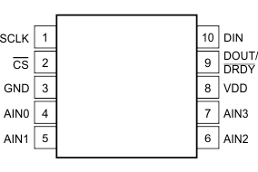
ADS1018-Q1 po_dgs_bas457.gif

Pin Functions

PIN TYPE DESCRIPTION
NO. NAME
1 SCLK Digital input Serial clock input
2 CS Digital input Chip select; active low. Connect to GND if not used.
3 GND Supply Ground
4 AIN0 Analog input Analog input 0. Leave unconnected or tie to VDD if not used.
5 AIN1 Analog input Analog input 1. Leave unconnected or tie to VDD if not used.
6 AIN2 Analog input Analog input 2. Leave unconnected or tie to VDD if not used.
7 AIN3 Analog input Analog input 3. Leave unconnected or tie to VDD if not used.
8 VDD Supply Power supply. Connect a 0.1-µF power supply decoupling capacitor to GND.
9 DOUT/DRDY Digital output Serial data output combined with data ready; active low
10 DIN Digital input Serial data input