ZHCS311D May   2009  – January 2018 ADS1113 , ADS1114 , ADS1115

PRODUCTION DATA.  

  1. 特性
  2. 应用
  3. 说明
    1.     Device Images
      1.      简化的方框图
  4. Revision History
  5. Device Comparison Table
  6. Pin Configuration and Functions
    1.     Pin Functions
  7. Specifications
    1. 7.1 Absolute Maximum Ratings
    2. 7.2 ESD Ratings
    3. 7.3 Recommended Operating Conditions
    4. 7.4 Thermal Information
    5. 7.5 Electrical Characteristics
    6. 7.6 Timing Requirements: I2C
    7. 7.7 Typical Characteristics
  8. Parameter Measurement Information
    1. 8.1 Noise Performance
  9. Detailed Description
    1. 9.1 Overview
    2. 9.2 Functional Block Diagrams
    3. 9.3 Feature Description
      1. 9.3.1 Multiplexer
      2. 9.3.2 Analog Inputs
      3. 9.3.3 Full-Scale Range (FSR) and LSB Size
      4. 9.3.4 Voltage Reference
      5. 9.3.5 Oscillator
      6. 9.3.6 Output Data Rate and Conversion Time
      7. 9.3.7 Digital Comparator (ADS1114 and ADS1115 Only)
      8. 9.3.8 Conversion Ready Pin (ADS1114 and ADS1115 Only)
      9. 9.3.9 SMbus Alert Response
    4. 9.4 Device Functional Modes
      1. 9.4.1 Reset and Power-Up
      2. 9.4.2 Operating Modes
        1. 9.4.2.1 Single-Shot Mode
        2. 9.4.2.2 Continuous-Conversion Mode
      3. 9.4.3 Duty Cycling For Low Power
    5. 9.5 Programming
      1. 9.5.1 I2C Interface
        1. 9.5.1.1 I2C Address Selection
        2. 9.5.1.2 I2C General Call
        3. 9.5.1.3 I2C Speed Modes
      2. 9.5.2 Slave Mode Operations
        1. 9.5.2.1 Receive Mode
        2. 9.5.2.2 Transmit Mode
      3. 9.5.3 Writing To and Reading From the Registers
      4. 9.5.4 Data Format
    6. 9.6 Register Map
      1. 9.6.1 Address Pointer Register (address = N/A) [reset = N/A]
        1. Table 6. Address Pointer Register Field Descriptions
      2. 9.6.2 Conversion Register (P[1:0] = 0h) [reset = 0000h]
        1. Table 7. Conversion Register Field Descriptions
      3. 9.6.3 Config Register (P[1:0] = 1h) [reset = 8583h]
        1. Table 8. Config Register Field Descriptions
      4. 9.6.4 Lo_thresh (P[1:0] = 2h) [reset = 8000h] and Hi_thresh (P[1:0] = 3h) [reset = 7FFFh] Registers
        1. Table 9. Lo_thresh and Hi_thresh Register Field Descriptions
  10. 10Application and Implementation
    1. 10.1 Application Information
      1. 10.1.1 Basic Connections
      2. 10.1.2 Single-Ended Inputs
      3. 10.1.3 Input Protection
      4. 10.1.4 Unused Inputs and Outputs
      5. 10.1.5 Analog Input Filtering
      6. 10.1.6 Connecting Multiple Devices
      7. 10.1.7 Quickstart Guide
    2. 10.2 Typical Application
      1. 10.2.1 Design Requirements
      2. 10.2.2 Detailed Design Procedure
        1. 10.2.2.1 Shunt Resistor Considerations
        2. 10.2.2.2 Operational Amplifier Considerations
        3. 10.2.2.3 ADC Input Common-Mode Considerations
        4. 10.2.2.4 Resistor (R1, R2, R3, R4) Considerations
        5. 10.2.2.5 Noise and Input Impedance Considerations
        6. 10.2.2.6 First-order RC Filter Considerations
        7. 10.2.2.7 Circuit Implementation
        8. 10.2.2.8 Results Summary
      3. 10.2.3 Application Curves
  11. 11Power Supply Recommendations
    1. 11.1 Power-Supply Sequencing
    2. 11.2 Power-Supply Decoupling
  12. 12Layout
    1. 12.1 Layout Guidelines
    2. 12.2 Layout Example
  13. 13器件和文档支持
    1. 13.1 Documentation Support
      1. 13.1.1 相关文档
    2. 13.2 相关链接
    3. 13.3 Receiving Notification of Documentation Updates
    4. 13.4 社区资源
    5. 13.5 商标
    6. 13.6 静电放电警告
    7. 13.7 Glossary
  14. 14机械、封装和可订购信息

封装选项

机械数据 (封装 | 引脚)
散热焊盘机械数据 (封装 | 引脚)
订购信息

Typical Characteristics

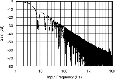
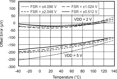
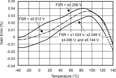
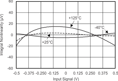
at TA = 25°C, VDD = 3.3 V, FSR = ±2.048 V, DR = 8 SPS (unless otherwise noted)
ADS1113 ADS1114 ADS1115 tc_ivdd-tmp_bas444.gif
Figure 2. Operating Current vs Temperature
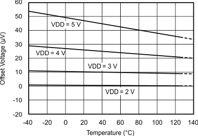
ADS1113 ADS1114 ADS1115 tc_oerr_1end-tmp_bas444.gif
Figure 4. Single-Ended Offset Error vs Temperature
ADS1113 ADS1114 ADS1115 tc_gerr-tmp_bas444.gif
Figure 6. Gain Error vs Temperature
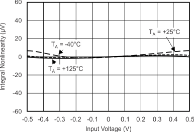
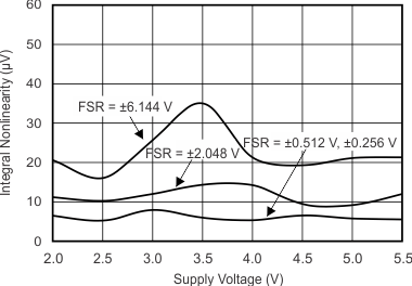
ADS1113 ADS1114 ADS1115 tc_inl-vs_bas444.gif
Figure 8. INL vs Supply Voltage
ADS1113 ADS1114 ADS1115 tc_inl-in_sig_fs512_bas444.gif
VDD = 3.3 V, FSR = ±0.512 V, DR = 8 SPS, best fit
Figure 10. INL vs Input Signal
ADS1113 ADS1114 ADS1115 tc_inl-insig_1024fsr_bas444.gif
VDD = 5 V, FSR = ±0.512 V, DR = 8 SPS, best fit
Figure 12. INL vs Input Signal
ADS1113 ADS1114 ADS1115 tc_noise-sig_bas444.gif
FSR = ±0.512 V
Figure 14. Noise vs Input Signal
ADS1113 ADS1114 ADS1115 tc_noise-tmp_bas444.gif
FSR = ±2.048 V, DR = 8 SPS
Figure 16. Noise vs Temperature
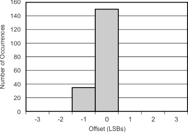
ADS1113 ADS1114 ADS1115 tc_histo_offset_bas444.gif
FSR = ±2.048 V, 185 units
Figure 18. Offset Histogram
ADS1113 ADS1114 ADS1115 tc_drate-tmp_bas444.gif
Figure 20. Data Rate vs Temperature
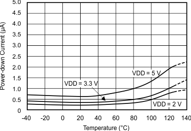
ADS1113 ADS1114 ADS1115 tc_iq-tmp_bas444.gif
Figure 3. Power-Down Current vs Temperature
ADS1113 ADS1114 ADS1115 tc_diff_oset-tmp_bas444.gif
Figure 5. Differential Offset vs Temperature
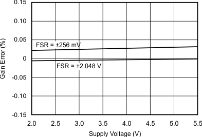
ADS1113 ADS1114 ADS1115 tc_gerr-vs_bas444.gif
Figure 7. Gain Error vs Supply Voltage
ADS1113 ADS1114 ADS1115 tc_inl-in_sig_fs2048_bas444.gif
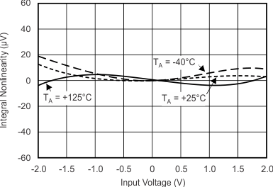
VDD = 3.3 V, FSR = ±2.048 V, DR = 8 SPS, best fit
Figure 9. INL vs Input Signal
ADS1113 ADS1114 ADS1115 tc_inl-insig_4096fsr_bas444.gif
VDD = 5 V, FSR = ±2.048 V, DR = 8 SPS, best fit
Figure 11. INL vs Input Signal
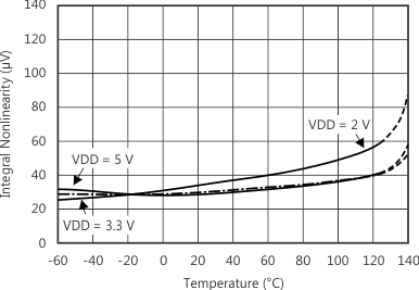
ADS1113 ADS1114 ADS1115 tc_inl-tmp_bas444.gif
Figure 13. INL vs Temperature
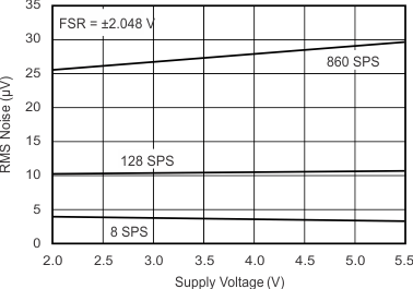
ADS1113 ADS1114 ADS1115 tc_noise-vs_bas444.gif
FSR = ±2.048 V
Figure 15. Noise vs Supply Voltage
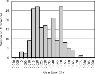
ADS1113 ADS1114 ADS1115 tc_histo_gerr_bas444.gif
FSR = ±2.048 V, 185 units
Figure 17. Gain Error Histogram
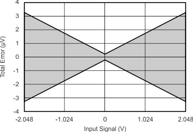
ADS1113 ADS1114 ADS1115 tc_terr-sig_bas444.gif
Differential inputs; includes noise, offset and gain error
Figure 19. Total Error vs Input Signal
ADS1113 ADS1114 ADS1115 tc_fresp_bas444.gif
DR = 8 SPS
Figure 21. Digital Filter Frequency Response