ZHCSEB1A October 2015 – November 2015 ADS1118-Q1
PRODUCTION DATA.
- 1 特性
- 2 应用
- 3 说明
- 4 修订历史记录
- 5 Device Comparison Table
- 6 Pin Configuration and Functions
- 7 Specifications
- 8 Parameter Measurement Information
- 9 Detailed Description
- 10Application and Implementation
- 11Power-Supply Recommendations
- 12Layout
- 13器件和文档支持
- 14机械、封装和可订购信息
12 Layout
12.1 Layout Guidelines
Use best design practices when laying out a printed-circuit-board (PCB) for both analog and digital components. This recommendation generally means that the layout separates analog components [such as ADCs, amplifiers, references, digital-to-analog converters (DACs), and analog muxes] from digital components [such as microcontrollers, complex programmable logic devices (CPLDs), field-programmable gate arrays (FPGAs), radio frequency (RF) transceivers, universal serial bus (USB) transceivers, and switching regulators]. An example of good component placement is shown in Figure 49. Although Figure 49 provides a good example of component placement, the best placement for each application is unique to the geometries, components, and PCB fabrication capabilities employed. That is, there is no single layout that is perfect for every design and careful consideration must always be used when designing with any analog component.
 Figure 49. System Component Placement
The use of split analog and digital ground planes is not necessary for improved noise performance (although for thermal isolation this option is a worthwhile consideration). However, the use of a solid ground plane or ground fill in PCB areas with no components is essential for optimum performance. If the system being used employs a split digital and analog ground plane, TI generally recommends that the ground planes be connected together as close to the device as possible. A two-layer board is possible using common grounds for both analog and digital grounds. Additional layers can be added to simplify PCB trace routing. Ground fill may also reduce EMI and RFI issues.
For best system performance, keep digital components, especially RF portions, as far as practically possible from analog circuitry in a given system. Additionally, minimize the distance that digital control traces run through analog areas and avoid placing these traces near sensitive analog components. Digital return currents usually flow through a ground path that is as close to the digital path as possible. If a solid ground connection to a plane is not available, these currents may find paths back to the source that interfere with analog performance. The implications that layout has on the temperature-sensing functions are much more significant than for ADC functions.
Bypass supply pins to ground with a low-ESR ceramic capacitor. The optimum placement of the bypass capacitors is as close as possible to the supply pins. The ground-side connections of the bypass capacitors must be low-impedance connections for optimum performance. The supply current flows through the bypass capacitor terminal first and then to the supply pin to make the bypassing most effective.
Analog inputs with differential connections must have a capacitor placed differentially across the inputs. Use high-quality differential capacitors. The best ceramic-chip capacitors are C0G (NPO), with stable properties and low-noise characteristics. Thermally isolate a copper region around the thermocouple input connections to create a thermally-stable cold junction. Obtaining acceptable performance with alternate layout schemes is possible as long as the above guidelines are followed.
12.2 Layout Example
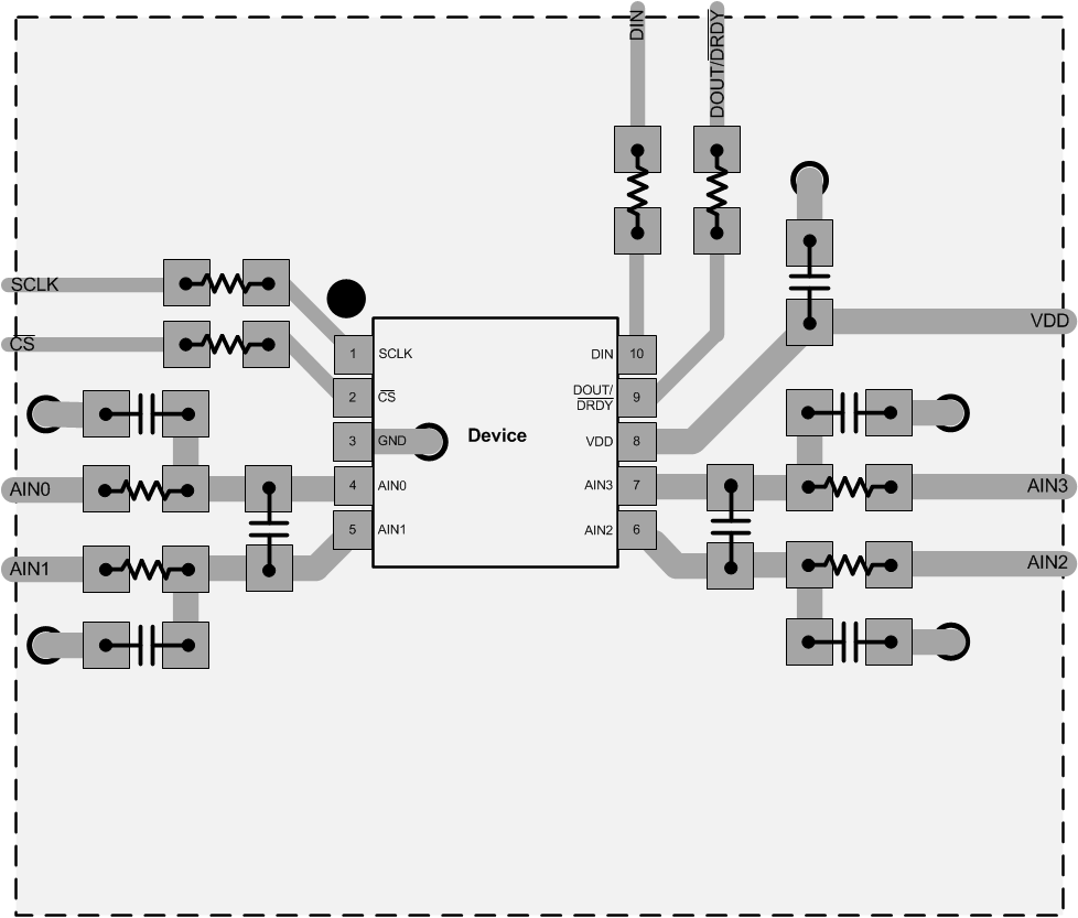
 Figure 50. VSSOP Package