ZHCSEB1A October 2015 – November 2015 ADS1118-Q1
PRODUCTION DATA.
- 1 特性
- 2 应用
- 3 说明
- 4 修订历史记录
- 5 Device Comparison Table
- 6 Pin Configuration and Functions
- 7 Specifications
- 8 Parameter Measurement Information
- 9 Detailed Description
- 10Application and Implementation
- 11Power-Supply Recommendations
- 12Layout
- 13器件和文档支持
- 14机械、封装和可订购信息
7 Specifications
7.1 Absolute Maximum Ratings
over operating ambient temperature range (unless otherwise noted)(1)| MIN | MAX | UNIT | ||
|---|---|---|---|---|
| Power-supply voltage | VDD to GND | –0.3 | 5.5 | V |
| Analog input voltage | AIN0, AIN1, AIN2, AIN3 | GND – 0.3 | VDD + 0.3 | V |
| Digital input voltage | DIN, DOUT/DRDY, SCLK, CS | GND – 0.3 | VDD + 0.3 | V |
| Input current, continuous | Any pin except power supply pins | –10 | 10 | mA |
| Temperature | Junction, TJ | –40 | 150 | °C |
| Storage, Tstg | –60 | 150 | ||
(1) Stresses beyond those listed under Absolute Maximum Ratings may cause permanent damage to the device. These are stress ratings only, which do not imply functional operation of the device at these or any other conditions beyond those indicated under Recommended Operating Conditions. Exposure to absolute-maximum-rated conditions for extended periods may affect device reliability.
7.2 ESD Ratings
| VALUE | UNIT | |||
|---|---|---|---|---|
| V(ESD) | Electrostatic discharge | Human body model (HBM), per AEC Q100-002(1) | ±2000 | V |
| Charged device model (CDM), per AEC Q100-011 | ±1000 | |||
(1) AEC Q100-002 indicates HBM stressing is done in accordance with the ANSI/ESDA/JEDEC JS-001 specification.
7.3 Recommended Operating Conditions
over operating ambient temperature range (unless otherwise noted)| MIN | NOM | MAX | UNIT | |||
|---|---|---|---|---|---|---|
| POWER SUPPLY | ||||||
| VDD | Power supply | VDD to GND | 2 | 5.5 | V | |
| ANALOG INPUTS(2) | ||||||
| FSR | Full-scale input voltage(1) | VIN = V(AINP) - V(AINN) | See Table 3 | |||
| V(AINx) | Absolute input voltage | GND | VDD | V | ||
| DIGITAL INPUTS | ||||||
| Input voltage | GND | VDD | V | |||
| TEMPERATURE | ||||||
| TA | Operating ambient temperature | –40 | 125 | °C | ||
(1) This parameter expresses the full-scale range of the ADC scaling. No more than VDD + 0.3 V or 5.5 V (whichever is smaller) must be applied to this device.
(2) AINP and AINN denote the selected positive and negative inputs. AINx denotes one of the four available analog inputs.
7.4 Thermal Information
| THERMAL METRIC(1) | ADS1118-Q1 | UNIT | |
|---|---|---|---|
| DGS (VSSOP) | |||
| 10 PINS | |||
| RθJA | Junction-to-ambient thermal resistance | 186.8 | °C/W |
| RθJC(top) | Junction-to-case (top) thermal resistance | 51.5 | °C/W |
| RθJB | Junction-to-board thermal resistance | 108.4 | °C/W |
| ψJT | Junction-to-top characterization parameter | 2.7 | °C/W |
| ψJB | Junction-to-board characterization parameter | 106.5 | °C/W |
| RθJC(bot) | Junction-to-case (bottom) thermal resistance | N/A | °C/W |
(1) For more information about traditional and new thermal metrics, see the Semiconductor and IC Package Thermal Metrics application report, SPRA953.
7.5 Electrical Characteristics
Maximum and minimum specifications apply from TA = –40°C to +125°C. Typical specifications are at TA = 25°C.All specifications are at VDD = 3.3 V, data rate = 8 SPS, and FSR = ±2.048 V (unless otherwise noted).
| PARAMETER | TEST CONDITIONS | MIN | TYP | MAX | UNIT | |
|---|---|---|---|---|---|---|
| ANALOG INPUTS | ||||||
| Common-mode input impedance | FSR = ±6.144 V(1) | 8 | MΩ | |||
| FSR = ±4.096 V(1), FSR = ±2.048 V | 6 | |||||
| FSR = ±1.024 V | 3 | |||||
| FSR = ±0.512 V, FSR = ±0.256 V | 100 | |||||
| Differential input impedance | FSR = ±6.144 V(1) | 22 | MΩ | |||
| FSR = ±4.096 V(1) | 15 | |||||
| FSR = ±2.048 V | 4.9 | |||||
| FSR = ±1.024 V | 2.4 | |||||
| FSR = ±0.512 V, FSR = ±0.256 V | 710 | kΩ | ||||
| SYSTEM PERFORMANCE | ||||||
| Resolution (no missing codes) | 16 | Bits | ||||
| DR | Data rate | 8, 16, 32, 64, 128, 250, 475, 860 | SPS | |||
| Data rate variation | All data rates | –10% | 10% | |||
| Output noise | See Noise Performance section | |||||
| INL | Integral nonlinearity | DR = 8 SPS, FSR = ±2.048 V(1) | 1 | LSB | ||
| Offset error | FSR = ±2.048 V, differential inputs | ±0.1 | ±2 | LSB | ||
| FSR = ±2.048 V, single-ended inputs | ±0.25 | |||||
| Offset drift | FSR = ±2.048 V | 0.002 | LSB/°C | |||
| Offset power-supply rejection | FSR = ±2.048 V, dc supply variation | 0.2 | LSB/V | |||
| Offset channel match | Match between any two inputs | 0.6 | LSB | |||
| Gain error(2) | FSR = ±2.048 V, TA = 25°C | 0.01% | 0.15% | |||
| Gain drift(2)(3) | FSR = ±0.256 V | 7 | ppm/°C | |||
| FSR = ±2.048 V | 5 | 40 | ||||
| FSR = ±6.144 V(1) | 5 | |||||
| Gain power-supply rejection | 10 | ppm/V | ||||
| Gain match(2) | Match between any two gains | 0.01% | 0.1% | |||
| Gain channel match | Match between any two inputs | 0.01% | 0.1% | |||
| CMRR | Common-mode rejection ratio | At DC, FSR = ±0.256 V | 105 | dB | ||
| At DC, FSR = ±2.048 V | 100 | |||||
| At DC, FSR = ±6.144 V(1) | 90 | |||||
| fCM = 50 Hz, DR = 860 SPS | 105 | |||||
| fCM = 60 Hz, DR = 860 SPS | 105 | |||||
| TEMPERATURE SENSOR | ||||||
| Temperature range | –40 | 125 | °C | |||
| Temperature resolution | 0.03125 | °C/LSB | ||||
| Accuracy | TA = 0°C to 70°C | 0.2 | ±1 | °C | ||
| TA = –40°C to +125°C | 0.4 | ±2 | ||||
| vs supply | 0.03125 | ±0.25 | °C/V | |||
| DIGITAL INPUTS/OUTPUTS | ||||||
| VIH | High-level input voltage | 0.7 VDD | VDD | V | ||
| VIL | Low-level input voltage | GND | 0.2 VDD | V | ||
| VOH | High-level output voltage | IOH = 1 mA | 0.8 VDD | V | ||
| VOL | Low-level output voltage | IOL = 1 mA | GND | 0.2 VDD | V | |
| IH | Input leakage, high | VIH = 5.5 V | –10 | 10 | μA | |
| IL | Input leakage, low | VIL = GND | –10 | 10 | μA | |
| POWER SUPPLY | ||||||
| IVDD | Supply current | Power-down, TA = 25°C | 0.5 | 2 | μA | |
| Power-down | 5 | |||||
| Operating, TA = 25°C | 150 | 200 | ||||
| Operating | 300 | |||||
| PD | Power dissipation | VDD = 5 V | 0.9 | mW | ||
| VDD = 3.3 V | 0.5 | |||||
| VDD = 2 V | 0.3 | |||||
(1) Best-fit INL; covers 99% of full-scale.
(2) Includes all errors from onboard PGA and voltage reference.
(3) Maximum value specified by characterization.
7.6 Timing Requirements: Serial Interface
over operating ambient temperature range and VDD = 2 V to 5.5 V (unless otherwise noted)| MIN | MAX | UNIT | ||
|---|---|---|---|---|
| tCSSC | Delay time, CS falling edge to first SCLK rising edge(1) | 100 | ns | |
| tSCCS | Delay time, final SCLK falling edge to CS rising edge | 100 | ns | |
| tCSH | Pulse duration, CS high | 200 | ns | |
| tSCLK | SCLK period | 250 | ns | |
| tSPWH | Pulse duration, SCLK high | 100 | ns | |
| tSPWL | Pulse duration, SCLK low(2) | 100 | ns | |
| 28 | ms | |||
| tDIST | Setup time, DIN valid before SCLK falling edge | 50 | ns | |
| tDIHD | Hold time, DIN valid after SCLK falling edge | 50 | ns | |
| tDOHD | Hold time, SCLK rising edge to DOUT invalid | 0 | ns | |
(1) CS can be tied low permanently in case the serial bus is not shared with any other device.
(2) Holding SCLK low longer than 28 ms resets the SPI interface.
7.7 Switching Characteristics: Serial Interface
over operating ambient temperature range (unless otherwise noted)| PARAMETER | TEST CONDITIONS | MIN | TYP | MAX | UNIT | |
|---|---|---|---|---|---|---|
| tCSDOD | Propagation delay time, CS falling edge to DOUT driven |
DOUT load = 20 pF || 100 kΩ to GND | 100 | ns | ||
| tDOPD | Propagation delay time, SCLK rising edge to valid new DOUT |
DOUT load = 20 pF || 100 kΩ to GND | 0 | 50 | ns | |
| tCSDOZ | Propagation delay time, CS rising edge to DOUT high impedance |
DOUT load = 20 pF || 100 kΩ to GND | 100 | ns | ||
 Figure 1. Serial Interface Timing
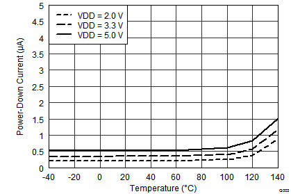
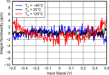
7.8 Typical Characteristics
at TA = 25°C, VDD = 3.3 V, and FSR = ±2.048 V (unless otherwise noted)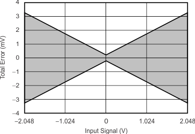
| DR = 860 SPS, diff Inputs; includes noise, offset, and gain errors |
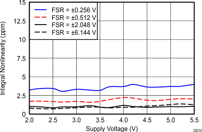
| FSR = ±0.512 V, DR = 8 SPS, VDD = 3.3 V, best fit |
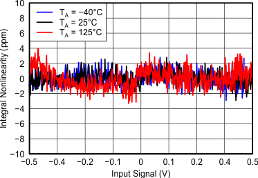
| FSR = ±0.512 V, DR = 8 SPS, VDD = 5 V, best fit | ||
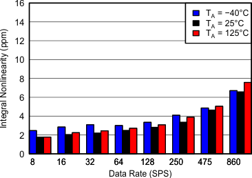
| FSR = ±2.048 V, best fit |
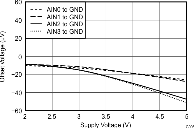
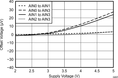
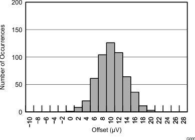
| FSR = ±2.048 V, | ||
| 540 units from 3 production lots |
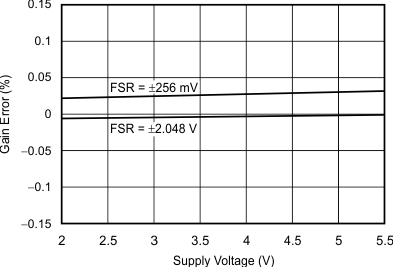
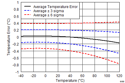
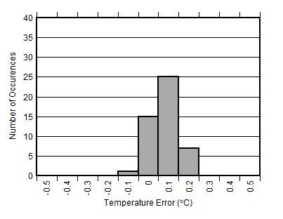
| TA = 0°C, 48 units from 3 production lots |
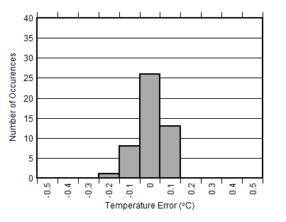
| TA = 70°C, 48 units from 3 production lots |
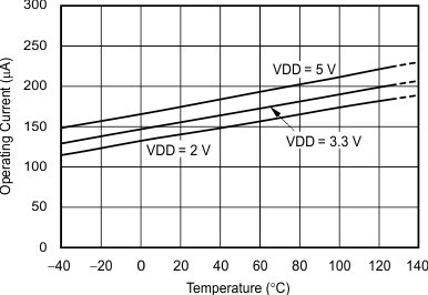
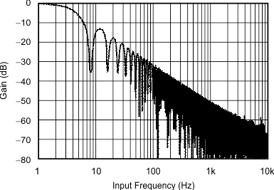
| DR = 8 SPS |
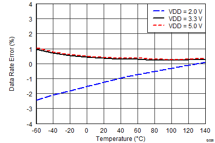
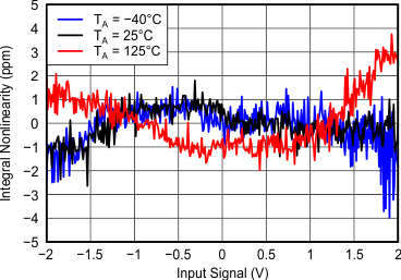
| FSR = ±2.048 V, DR = 8 SPS, VDD = 3.3 V, best fit |
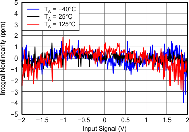
| FSR = ±2.048 V, DR = 8 SPS, VDD = 5 V, best fit |
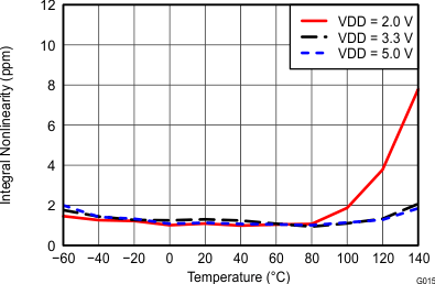
| FSR = ±2.048 V, DR = 8 SPS, best fit | ||
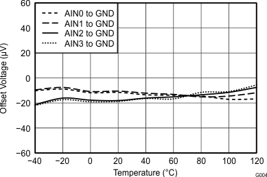
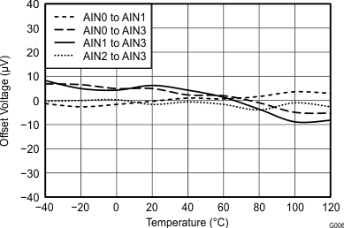
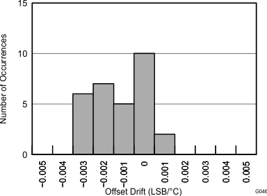
| FSR = ±2.048 V, TA = –40°C to +125°C, mux = AIN0 to AIN3, | ||
| 540 units from 3 production lots |
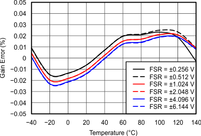
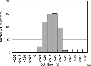
| FSR = ±2.048 V, 540 units from 3 production lots |

| TA = –40°C, 48 units from 3 production lots | ||
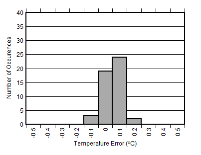
| TA = 25°C, 48 units from 3 production lots |
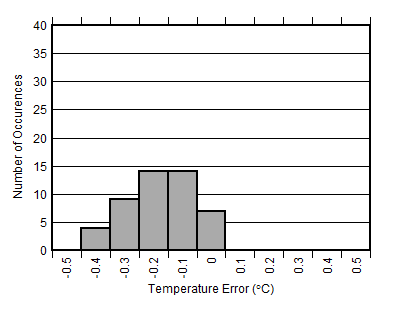
| TA = 125°C, 48 units from 3 production lots |
