ZHCSEE1F October   2010  – September 2019 ADS1118

PRODUCTION DATA.  

  1. 特性
  2. 应用
  3. 说明
    1.     Device Images
      1.      K 型热电偶测量使用集成温度传感器进行冷结点补偿
  4. 修订历史记录
  5. Device Comparison Table
  6. Pin Configuration and Functions
    1.     Pin Functions
  7. Specifications
    1. 7.1 Absolute Maximum Ratings
    2. 7.2 ESD Ratings
    3. 7.3 Recommended Operating Conditions
    4. 7.4 Thermal Information
    5. 7.5 Electrical Characteristics
    6. 7.6 Timing Requirements: Serial Interface
    7. 7.7 Switching Characteristics: Serial Interface
    8. 7.8 Typical Characteristics
  8. Parameter Measurement Information
    1. 8.1 Noise Performance
  9. Detailed Description
    1. 9.1 Overview
    2. 9.2 Functional Block Diagram
    3. 9.3 Feature Description
      1. 9.3.1 Multiplexer
      2. 9.3.2 Analog Inputs
      3. 9.3.3 Full-Scale Range (FSR) and LSB Size
      4. 9.3.4 Voltage Reference
      5. 9.3.5 Oscillator
      6. 9.3.6 Temperature Sensor
        1. 9.3.6.1 Converting from Temperature to Digital Codes
        2. 9.3.6.2 Converting from Digital Codes to Temperature
    4. 9.4 Device Functional Modes
      1. 9.4.1 Reset and Power Up
      2. 9.4.2 Operating Modes
        1. 9.4.2.1 Single-Shot Mode and Power-Down
        2. 9.4.2.2 Continuous-Conversion Mode
      3. 9.4.3 Duty Cycling for Low Power
    5. 9.5 Programming
      1. 9.5.1 Serial Interface
      2. 9.5.2 Chip Select (CS)
      3. 9.5.3 Serial Clock (SCLK)
      4. 9.5.4 Data Input (DIN)
      5. 9.5.5 Data Output and Data Ready (DOUT/DRDY)
      6. 9.5.6 Data Format
      7. 9.5.7 Data Retrieval
        1. 9.5.7.1 32-Bit Data Transmission Cycle
        2. 9.5.7.2 16-Bit Data Transmission Cycle
    6. 9.6 Register Maps
      1. 9.6.1 Conversion Register [reset = 0000h]
        1. Table 6. Conversion Register Field Descriptions
      2. 9.6.2 Config Register [reset = 058Bh]
        1. Table 7. Config Register Field Descriptions
  10. 10Application and Implementation
    1. 10.1 Application Information
      1. 10.1.1 Serial Interface Connections
      2. 10.1.2 GPIO Ports for Communication
      3. 10.1.3 Analog Input Filtering
      4. 10.1.4 Single-Ended Inputs
      5. 10.1.5 Connecting Multiple Devices
      6. 10.1.6 Pseudo Code Example
    2. 10.2 Typical Application
      1. 10.2.1 Design Requirements
      2. 10.2.2 Detailed Design Procedure
      3. 10.2.3 Application Curves
  11. 11Power Supply Recommendations
    1. 11.1 Power-Supply Sequencing
    2. 11.2 Power-Supply Decoupling
  12. 12Layout
    1. 12.1 Layout Guidelines
    2. 12.2 Layout Example
  13. 13器件和文档支持
    1. 13.1 文档支持
      1. 13.1.1 相关文档
    2. 13.2 接收文档更新通知
    3. 13.3 社区资源
    4. 13.4 商标
    5. 13.5 静电放电警告
    6. 13.6 Glossary
  14. 14机械、封装和可订购信息

封装选项

机械数据 (封装 | 引脚)
散热焊盘机械数据 (封装 | 引脚)
订购信息

Power-Supply Decoupling

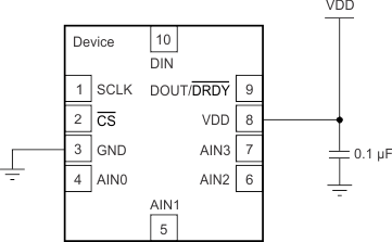
Good power-supply decoupling is important to achieve optimum performance. VDD must be decoupled with at least a 0.1-µF capacitor, as shown in Figure 54. The 0.1-μF bypass capacitor supplies the momentary bursts of extra current required from the supply when the ADS1118 is converting. Place the bypass capacitor as close to the power-supply pin of the device as possible using low-impedance connections. TI recommends using multi-layer ceramic chip capacitors (MLCCs) that offer low equivalent series resistance (ESR) and inductance (ESL) characteristics for power-supply decoupling purposes. For very sensitive systems, or for systems in harsh noise environments, avoiding the use of vias for connecting the capacitors to the device pins may offer superior noise immunity. The use of multiple vias in parallel lowers the overall inductance and is beneficial for connections to ground planes.
ADS1118 ai_1end_inputs_bas457.gifFigure 54. Power Supply Decoupling