ZHCSDB9C August 2013 – February 2017 ADS1120
PRODUCTION DATA.
- 1 特性
- 2 应用
- 3 说明
- 4 修订历史记录
- 5 Pin Configuration and Functions
- 6 Specifications
- 7 Parameter Measurement Information
-
8 Detailed Description
- 8.1 Overview
- 8.2 Functional Block Diagram
- 8.3 Feature Description
- 8.4 Device Functional Modes
- 8.5 Programming
- 8.6 Register Map
- 9 Application and Implementation
- 10Power Supply Recommendations
- 11Layout
- 12器件和文档支持
- 13机械、封装和可订购信息
封装选项
机械数据 (封装 | 引脚)
散热焊盘机械数据 (封装 | 引脚)
- RVA|16
订购信息
9 Application and Implementation
NOTE
Information in the following applications sections is not part of the TI component specification, and TI does not warrant its accuracy or completeness. TI’s customers are responsible for determining suitability of components for their purposes. Customers should validate and test their design implementation to confirm system functionality.
9.1 Application Information
The ADS1120 is a precision, 16-bit, ΔΣ ADC that offers many integrated features to ease the measurement of the most common sensor types including various types of temperature and bridge sensors. Primary considerations when designing an application with the ADS1120 include analog input filtering, establishing an appropriate external reference for ratiometric measurements, and setting the common-mode input voltage for the internal PGA. Connecting and configuring the serial interface appropriately is another concern. These considerations are discussed in the following sections.
9.1.1 Serial Interface Connections
The principle serial interface connections for the ADS1120 are shown in Figure 72.
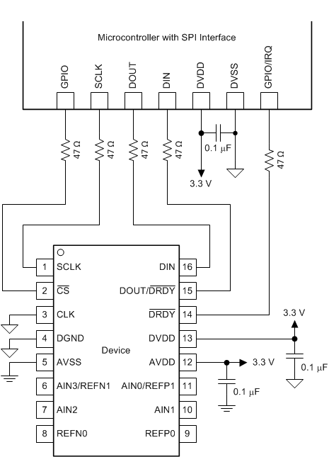 Figure 72. Serial Interface Connections
Most microcontroller SPI peripherals can operate with the ADS1120. The interface operates in SPI mode 1 where CPOL = 0 and CPHA = 1. In SPI mode 1, SCLK idles low and data are launched or changed only on SCLK rising edges; data are latched or read by the master and slave on SCLK falling edges. Details of the SPI communication protocol employed by the device can be found in the SPI Timing Requirements section.
TI recommends placing 47-Ω resistors in series with all digital input and output pins (CS, SCLK, DIN, DOUT/DRDY, and DRDY). This resistance smooths sharp transitions, suppresses overshoot, and offers some overvoltage protection. Care must be taken to meet all SPI timing requirements because the additional resistors interact with the bus capacitances present on the digital signal lines.
9.1.2 Analog Input Filtering
Analog input filtering serves two purposes: first, to limit the effect of aliasing during the sampling process and second, to reduce external noise from being a part of the measurement.
As with any sampled system, aliasing can occur if proper antialias filtering is not in place. Aliasing occurs when frequency components are present in the input signal that are higher than half the sampling frequency of the ADC (also known as the Nyquist frequency). These frequency components are folded back and show up in the actual frequency band of interest below half the sampling frequency. Note that inside a ΔΣ ADC, the input signal is sampled at the modulator frequency f(MOD) and not at the output data rate. The filter response of the digital filter repeats at multiples of the sampling frequency (f(MOD)), as shown in Figure 73. Signals or noise up to a frequency where the filter response repeats are attenuated to a certain amount by the digital filter depending on the filter architecture. Any frequency components present in the input signal around the modulator frequency or multiples thereof are not attenuated and alias back into the band of interest, unless attenuated by an external analog filter.
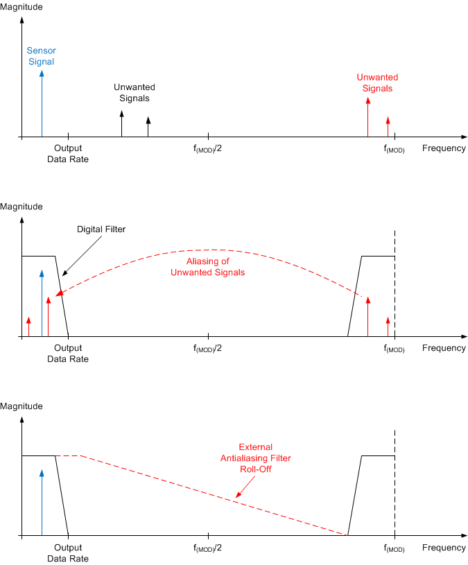 Figure 73. Effect of Aliasing
Many sensor signals are inherently bandlimited; for example, the output of a thermocouple has a limited rate of change. In this case the sensor signal does not alias back into the pass-band when using a ΔΣ ADC. However, any noise pick-up along the sensor wiring or the application circuitry can potentially alias into the pass-band. Power line-cycle frequency and harmonics are one common noise source. External noise can also be generated from electromagnetic interference (EMI) or radio frequency interference (RFI) sources, such as nearby motors and cellular phones. Another noise source typically exists on the printed circuit board (PCB) itself in the form of clocks and other digital signals. Analog input filtering helps remove unwanted signals from affecting the measurement result.
A first-order resistor-capacitor (RC) filter is (in most cases) sufficient to either totally eliminate aliasing, or to reduce the effect of aliasing to a level within the noise floor of the sensor. Ideally, any signal beyond f(MOD) / 2 is attenuated to a level below the noise floor of the ADC. The digital filter of the ADS1120 attenuates signals to a certain degree, as illustrated in the filter response plots in the Digital Filter section. In addition, noise components are usually smaller in magnitude than the actual sensor signal. Therefore, using a first-order RC filter with a cutoff frequency set at the output data rate or 10x higher is generally a good starting point for a system design.
Internal to the device, prior to the PGA inputs, is an EMI filter as shown in Figure 39. The cutoff frequency of this filter is approximately 31.8 MHz, which helps reject high-frequency interferences.
9.1.3 External Reference and Ratiometric Measurements
The full-scale range of the ADS1120 is defined by the reference voltage and the PGA gain (FSR = ±Vref / Gain). An external reference can be used instead of the integrated 2.048-V reference to adapt the FSR to the specific system needs. An external reference must be used if VIN > 2.048 V. For example, an external 5-V reference and an AVDD = 5 V are required in order to measure a single-ended signal that can swing between 0 V and 5 V.
The reference inputs of the device also allow the implementation of ratiometric measurements. In a ratiometric measurement the same excitation source that is used to excite the sensor is also used to establish the reference for the ADC. As an example, a simple form of a ratiometric measurement uses the same current source to excite both the resistive sensor element (such as an RTD) and another resistive reference element that is in series with the element being measured. The voltage that develops across the reference element is used as the reference source for the ADC. Because current noise and drift are common to both the sensor measurement and the reference, these components cancel out in the ADC transfer function. The output code is only a ratio of the sensor element and the value of the reference resistor. The value of the excitation current source itself is not part of the ADC transfer function.
9.1.4 Establishing a Proper Common-Mode Input Voltage
The ADS1120 can be used to measure various types of input signal configurations: single-ended, pseudo-differential, and fully-differential signals (which can be either unipolar or bipolar). However, configuring the device properly for the respective signal type is important.
Signals where the negative analog input is fixed and referenced to analog ground (V(AINN) = 0 V) are commonly called single-ended signals. The common-mode voltage of a single-ended signal consequently varies between 0 V and VIN / 2. If the PGA is disabled and bypassed, the common-mode input voltage of the ADS1120 can be as low as 100 mV below AVSS and as large as 100 mV above AVDD. Therefore, the PGA_BYPASS bit must be set in order to measure single-ended signals when a unipolar analog supply is used (AVSS = 0 V). Gains of 1, 2, and 4 are still possible in this configuration. Measuring a 0-mA to 20-mA or 4-mA to 20-mA signal across a load resistor of 100 Ω referenced to GND is a typical example. The ADS1120 can directly measure the signal across the load resistor using a unipolar supply, the internal 2.048-V reference, and gain = 1 when the PGA is bypassed.
If gains larger than 4 are needed to measure a single-ended signal, the PGA must be enabled. In this case, a bipolar supply is required for the ADS1120 to meet the common-mode voltage requirement of the PGA.
Signals where the negative analog input (AINN) is fixed at a voltage other the 0 V are referred to as pseudo-differential signals. The common-mode voltage of a pseudo-differential signal varies between V(AINN) and V(AINN) + VIN / 2.
Fully-differential signals in contrast are defined as signals having a constant common-mode voltage where the positive and negative analog inputs swing 180° out-of-phase but have the same amplitude.
The ADS1120 can measure pseudo-differential and fully-differential signals both with the PGA enabled or bypassed. However, the PGA must be enabled in order to use gains greater than 4. The common-mode voltage of the input signal must meet the input-common mode voltage restrictions of the PGA (as explained in the PGA Common-Mode Voltage Requirements section) when the PGA is enabled. Setting the common-mode voltage at or near (AVSS + AVDD) / 2 in most cases satisfies the PGA common-mode voltage requirements.
Signals where both the positive and negative inputs are always ≥ 0 V are called unipolar signals. These signals can in general be measured with the ADS1120 using a unipolar analog supply (AVSS = 0 V). As mentioned previously, the PGA must be bypassed in order to measure single-ended, unipolar signals when using a unipolar supply.
A signal is called bipolar when either the positive or negative input can swing below 0 V. A bipolar analog supply (such as AVDD = 2.5 V, AVSS = –2.5 V) is required in order to measure bipolar signals with the ADS1120. A typical application task is measuring a single-ended, bipolar ±10 V signal where AINN is fixed at 0 V while AINP swings between –10 V and 10 V. The ADS1120 cannot directly measure this signal because the 10 V exceeds the analog power-supply limits. However, one possible solution is to use a bipolar analog supply (AVDD = 2.5 V, AVSS = –2.5 V), gain = 1, and a resistor divider in front of the ADS1120. The resistor divider must divide the voltage down to ≤ ±2.048 V to be able to measure it using the internal 2.048-V reference.
9.1.5 Unused Inputs and Outputs
To minimize leakage currents on the analog inputs, leave unused analog and reference inputs floating, or connect the inputs to mid-supply or to AVDD. AIN3/REFN1 is an exception. Leave the AIN3/REFN1 pin floating when not used in order to avoid accidently shorting the pin to AVSS through the internal low-side switch. Connecting unused analog or reference inputs to AVSS is possible as well, but can yield higher leakage currents than the previously mentioned options.
Do not float unused digital inputs; excessive power-supply leakage current can result. Tie all unused digital inputs to the appropriate levels, DVDD or DGND, even when in power-down mode. If CS is not used, tie this pin to DGND. If the internal oscillator is used, tie the CLK pin to DGND. If the DRDY output is not used, leave the pin unconnected or tie the pin to DVDD using a weak pullup resistor.
9.1.6 Pseudo Code Example
The following list shows a pseudo code sequence with the required steps to set up the device and the microcontroller that interfaces to the ADC in order to take subsequent readings from the ADS1120 in continuous conversion mode. The dedicated DRDY pin is used to indicate availability of new conversion data. The default configuration register settings are changed to gain = 16, continuous conversion mode, and simultaneous 50-Hz and 60-Hz rejection.
| Power-up; Delay to allow power supplies to settle and power-up reset to complete; minimum of 50 µs; Configure the SPI interface of the microcontroller to SPI mode 1 (CPOL = 0, CPHA = 1); If the CS pin is not tied low permanently, configure the microcontroller GPIO connected to CS as an output; Configure the microcontroller GPIO connected to the DRDY pin as a falling edge triggered interrupt input; Set CS to the device low; Delay for a minimum of td(CSSC); Send the RESET command (06h) to make sure the device is properly reset after power-up; Delay for a minimum of 50 µs + 32 · t(CLK); Write the respective register configuration with the WREG command (43h, 08h, 04h, 10h, and 00h); As an optional sanity check, read back all configuration registers with the RREG command (23h); Send the START/SYNC command (08h) to start converting in continuous conversion mode; Delay for a minimum of td(SCCS); Clear CS to high (resets the serial interface); Loop |
|
| { Wait for DRDY to transition low; Take CS low; Delay for a minimum of td(CSSC); Send 16 SCLK rising edges to read out conversion data on DOUT/DRDY; Delay for for a minimum of td(SCCS); Clear CS to high; } |
|
| Take CS low; Delay for a minimum of td(CSSC); Send the POWERDOWN command (02h) to stop conversions and put the device in power-down mode; Delay for a minimum of td(SCCS); Clear CS to high; |
|
TI recommends running an offset calibration before performing any measurements or when changing the gain of the PGA. The internal offset of the device can, for example, be measured by shorting the inputs to mid-supply (MUX[3:1] = 1110). The microcontroller then takes multiple readings from the device with the inputs shorted and stores the average value in the microcontroller memory. When measuring the sensor signal, the microcontroller then subtracts the stored offset value from each device reading to obtain an offset compensated result. Note that the offset can be either positive or negative in value.
9.2 Typical Applications
9.2.1 K-Type Thermocouple Measurement (–200°C to +1250°C)
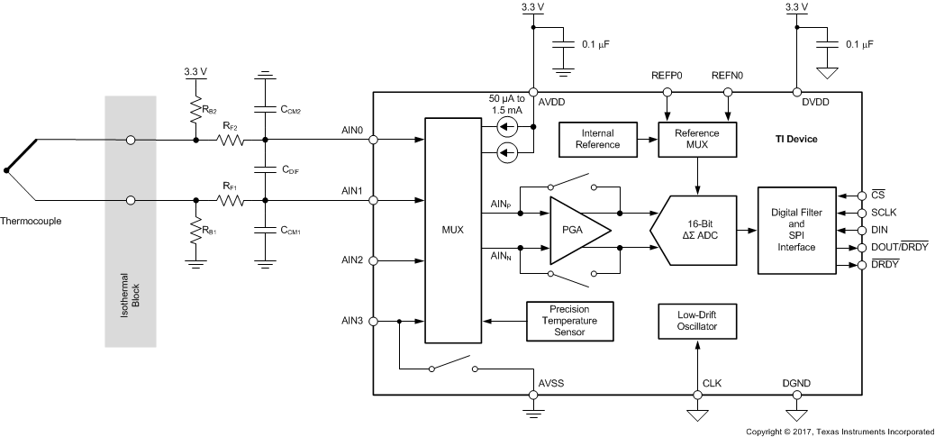
Figure 74 shows the basic connections of a thermocouple measurement system when using the internal high-precision temperature sensor for cold-junction compensation. Apart from the thermocouple itself, the only external circuitry required are two biasing resistors, a simple low-pass, antialiasing filter, and the power-supply decoupling capacitors.
9.2.1.1 Design Requirements
Table 21. Design Requirements
| DESIGN PARAMETER | VALUE |
|---|---|
| Supply voltage | 3.3 V |
| Reference voltage | Internal 2.048-V reference |
| Update rate | ≥10 readings per second |
| Thermocouple type | K |
| Temperature measurement range | –200°C to +1250°C |
| Measurement accuracy at TA = 25°C(1) | ±0.5°C |
offset calibration at T(TC) = T(CJ) = 25°C; no gain calibration.
9.2.1.2 Detailed Design Procedure
The biasing resistors RB1 and RB2 are used to set the common-mode voltage of the thermocouple to within the specified common-mode voltage range of the PGA (in this example, to mid-supply AVDD / 2). If the application requires the thermocouple to be biased to GND, either a bipolar supply (for example, AVDD = 2.5 V and AVSS = –2.5 V) must be used for the device to meet the common-mode voltage requirement of the PGA, or the PGA must be bypassed. When choosing the values of the biasing resistors, care must be taken so that the biasing current does not degrade measurement accuracy. The biasing current flows through the thermocouple and can cause self-heating and additional voltage drops across the thermocouple leads. Typical values for the biasing resistors range from 1 MΩ to 50 MΩ.
In addition to biasing the thermocouple, RB1 and RB2 are also useful for detecting an open thermocouple lead. When one of the thermocouple leads fails open, the biasing resistors pull the analog inputs (AIN0 and AIN1) to AVDD and AVSS, respectively. The ADC consequently reads a full-scale value, which is outside the normal measurement range of the thermocouple voltage, to indicate this failure condition.
Although the device digital filter attenuates high-frequency components of noise, TI recommends providing a first-order, passive RC filter at the inputs to further improve performance. The differential RC filter formed by RF1, RF2, and the differential capacitor CDIF offers a cutoff frequency that is calculated using Equation 17.
Two common-mode filter capacitors (CM1 and CM2) are also added to offer attenuation of high-frequency, common-mode noise components. TI recommends that the differential capacitor CDIF be at least an order of magnitude (10x) larger than the common-mode capacitors (CM1 and CM2) because mismatches in the common-mode capacitors can convert common-mode noise into differential noise.
The filter resistors RF1 and RF2 also serve as current-limiting resistors. These resistors limit the current into the analog inputs (AIN0 and AIN1) of the device to safe levels if an overvoltage on the inputs occur. Care must be taken when choosing the filter resistor values because the input currents flowing into and out of the device cause a voltage drop across the resistors. This voltage drop shows up as an additional offset error at the ADC inputs. TI recommends limiting the filter resistor values to below 1 kΩ.
The filter component values used in this design are: RF1 = RF2 = 1 kΩ, CDIF = 100 nF, and CCM1 = CCM2 = 10 nF.
The highest measurement resolution is achieved when matching the largest potential input signal to the FSR of the ADC by choosing the highest possible gain. From the design requirement, the maximum thermocouple voltage occurs at T(TC) = 1250°C and is V(TC) = 50.644 mV as defined in the tables published by the National Institute of Standards and Technology (NIST) using a cold-junction temperature of T(CJ) = 0°C. A thermocouple produces an output voltage that is proportional to the temperature difference between the thermocouple tip and the cold junction. If the cold junction is at a temperature below 0°C, the thermocouple produces a voltage larger than 50.644 mV. The isothermal block area is constrained by the operating temperature range of the device. Therefore, the isothermal block temperature is limited to –40°C. A K-type thermocouple at T(TC) = 1250°C produces an output voltage of V(TC) = 50.644 mV – (–1.527 mV) = 52.171 mV when referenced to a cold-junction temperature of T(CJ) = –40°C. The maximum gain that can be applied when using the internal 2.048-V reference is then calculated as (2.048 V / 52.171 mV) = 39.3. The next smaller PGA gain setting the device offers is 32.
The device integrates a high-precision temperature sensor that can be used to measure the temperature of the cold junction. To measure the internal temperature of the ADS1120, the device must be set to internal temperature sensor mode by setting the TS bit to 1 in the configuration register. For best performance, careful board layout is critical to achieve good thermal conductivity between the cold junction and the device package.
However, the device does not perform automatic cold-junction compensation of the thermocouple. This compensation must be done in the microcontroller that interfaces to the device. The microcontroller requests one or multiple readings of the thermocouple voltage from the device and then sets the device to internal temperature sensor mode (TS = 1) to acquire the temperature of the cold junction. An algorithm similar to the following must be implemented on the microcontroller to compensate for the cold-junction temperature:
- Measure the thermocouple voltage, V(TC), between AIN0 and AIN1.
- Measure the temperature of the cold junction, T(CJ), using the temperature sensor mode of the ADS1120.
- Convert the cold-junction temperature into an equivalent thermoelectric voltage, V(CJ), using the tables or equations provided by NIST.
- Add V(TC) and V(CJ) and translate the summation back into a thermocouple temperature using the NIST tables or equations again.
In some applications, the integrated temperature sensor of the ADS1120 cannot be used (for example, if the accuracy is not high enough or if the device cannot be placed close enough to the cold junction). The additional analog input channels of the device can be used in this case to measure the cold-junction temperature with a thermistor, RTD, or an analog temperature sensor.
The device is capable of 16-bit, noise-free resolution using a gain of 32, the internal 2.048-V reference, and a data rate of 20 SPS (see Table 1 and Table 2). Accordingly the device is able to resolve signals as small as one LSB. The LSB size is calculated using Equation 18:
To get an approximation of the achievable temperature resolution per ADC code, the LSB size is divided by the average sensitivity of a K-type thermocouple (41 µV/°C), as shown in Equation 19.
The register settings for this design are shown in Table 22.
Table 22. Register Settings
| REGISTER | SETTING | DESCRIPTION |
|---|---|---|
| 00h | 0Ah | AINP = AIN0, AINN = AIN1, gain = 32, PGA enabled |
| 01h | 04h | DR = 20 SPS, normal mode, continuous conversion mode |
| 02h | 10h | Internal voltage reference, simultaneous 50-Hz and 60-Hz rejection |
| 03h | 00h | No IDACs used |
9.2.1.3 Application Curves
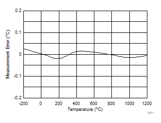
Figure 75 and Figure 76 show the measurement results. The measurements are taken at TA = T(CJ) = 25°C. A system offset calibration is performed at T(TC) = 25°C, which translates to a V(TC) = 0 V when T(CJ) = 25°C. No gain calibration is implemented. The data in Figure 75 are taken using a precision voltage source as the input signal instead of a thermocouple. The respective temperature measurement error in Figure 76 is calculated from the data in Figure 75 using the NIST tables.
The design meets the required temperature measurement accuracy given in Table 21. Note that the measurement error shown in Figure 76 does not include the error of the thermocouple itself and the measurement error of the cold-junction temperature. Those two error sources are in general larger than 0.2°C and therefore, in many cases, dominate the overall system measurement accuracy.

9.2.2 3-Wire RTD Measurement (–200°C to +850°C)
The ADS1120 integrates all necessary features (such as dual-matched programmable current sources, buffered reference inputs, and a PGA) to ease the implementation of ratiometric 2-, 3-, and 4-wire RTD measurements. Figure 77 shows a typical implementation of a ratiometric 3-wire RTD measurement using the excitation current sources integrated in the device to excite the RTD as well as to implement automatic RTD lead-resistance compensation.
9.2.2.1 Design Requirements
Table 23. Design Requirements
| DESIGN PARAMETER | VALUE |
|---|---|
| Supply voltage | 3.3 V |
| Update rate | 20 readings per second |
| RTD type | 3-wire Pt100 |
| Maximum RTD lead resistance | 15 Ω |
| RTD excitation current | 500 µA |
| Temperature measurement range | –200°C to +850°C |
| Measurement accuracy at TA = 25°C(1) | ±0.2°C |
offset calibration is performed with RRTD = 100 Ω; no gain calibration.
9.2.2.2 Detailed Design Procedure
The circuit in Figure 77 employs a ratiometric measurement approach. In other words, the sensor signal (that is, the voltage across the RTD in this case) and the reference voltage for the ADC are derived from the same excitation source. Therefore, errors resulting from temperature drift or noise of the excitation source cancel out because these errors are common to both the sensor signal and the reference.
In order to implement a ratiometric 3-wire RTD measurement using the device, IDAC1 is routed to one of the leads of the RTD and IDAC2 is routed to the second RTD lead. Both currents have the same value, which is programmable by the IDAC[2:0] bits in the configuration register. The design of the device ensures that both IDAC values are closely matched, even across temperature. The sum of both currents flows through a precision, low-drift reference resistor, RREF. The voltage, Vref, generated across the reference resistor (as shown in Equation 20) is used as the ADC reference voltage. Equation 20 reduces to Equation 21 because IIDAC1 = IIDAC2.
To simplify the following discussion, the individual lead resistance values of the RTD (RLEADx) are set to zero. Only IDAC1 excites the RTD to produce a voltage (VRTD) proportional to the temperature-dependable RTD value and the IDAC1 value, as shown in Equation 22.
The device internally amplifies the voltage across the RTD using the PGA and compares the resulting voltage against the reference voltage to produce a digital output code proportional to Equation 23 through Equation 25:
As can be seen from Equation 25, the output code only depends on the value of the RTD, the PGA gain, and the reference resistor (RREF), but not on the IDAC1 value. The absolute accuracy and temperature drift of the excitation current therefore does not matter. However, because the value of the reference resistor directly affects the measurement result, choosing a reference resistor with a very low temperature coefficient is important to limit errors introduced by the temperature drift of RREF.
The second IDAC2 is used to compensate for errors introduced by the voltage drop across the lead resistance of the RTD. All three leads of a 3-wire RTD typically have the same length and, thus, the same lead resistance. Also, IDAC1 and IDAC2 have the same value. Taking the lead resistance into account, the differential voltage (VIN) across the ADC inputs, AIN0 and AIN1, is calculated using Equation 26:
When RLEAD1 = RLEAD2 and IIDAC1 = IIDAC2, Equation 26 reduces to Equation 27:
In other words, the measurement error resulting from the voltage drop across the RTD lead resistance is compensated, as long as the lead resistance values and the IDAC values are well matched.
A first-order differential and common-mode RC filter (RF1, RF2, CDIF1, CCM1, and CCM2) is placed on the ADC inputs, as well as on the reference inputs (RF3, RF4, CDIF2, CCM3, and CCM4). The same guidelines for designing the input filter apply as described in the Thermocouple Measurement section. For best performance, TI recommends matching the corner frequencies of the input and reference filter. More detailed information on matching the input and reference filter can be found in application report RTD Ratiometric Measurements and Filtering Using the ADS1148 and ADS1248 (SBAA201).
The reference resistor RREF not only serves to generate the reference voltage for the device, but also sets the common-mode voltage of the RTD to within the specified common-mode voltage range of the PGA.
When designing the circuit, care must also be taken to meet the compliance voltage requirement of the IDACs. The IDACs require that the maximum voltage drop developed across the current path to AVSS be equal or less than AVDD – 0.9 V in order to operate accurately. This requirement means that Equation 28 must be met at all times.
The device also offers the possibility to route the IDACs to the same inputs used for measurement. If the filter resistor values RF1 and RF2 are small enough and well matched, IDAC1 can be routed to AIN1 and IDAC2 to AIN0 in Figure 77. In this manner, even two 3-wire RTDs sharing the same reference resistor can be measured with a single device.
This design example discusses the implementation of a 3-wire Pt100 measurement to be used to measure temperatures ranging from –200°C to +850°C as stated in Table 23. The excitation current for the Pt100 is chosen as IIDAC1 = 500 µA, which means a combined current of 1 mA is flowing through the reference resistor, RREF. As mentioned previously, besides creating the reference voltage for the ADS1120, the voltage across RREF also sets the common-mode voltage for the RTD measurement. In general, choose the largest reference voltage possible while still maintaining the compliance voltage of the IDACs as well as meeting the common-mode voltage requirement of the PGA. TI recommends setting the common-mode voltage at or near half the analog supply (in this case 3.3 V / 2 = 1.65 V), which in most cases satisfies the common-mode voltage requirements of the PGA. The value for RREF is then calculated by Equation 29:
The stability of RREF is critical to achieve good measurement accuracy over temperature and time. Choosing a reference resistor with a temperature coefficient of ±10 ppm/°C or better is advisable. If a 1.65 kΩ value is not readily available, another value near 1.65 kΩ (such as 1.62 kΩ or 1.69 kΩ) can certainly be used as well.
As a last step, the PGA gain must be selected in order to match the maximum input signal to the FSR of the ADC. The resistance of a Pt100 increases with temperature. Therefore, the maximum voltage to be measured (VIN (MAX)) occurs at the positive temperature extreme. At 850°C, a Pt100 has an equivalent resistance of approximately 391 Ω as per the NIST tables. The voltage across the Pt100 equates to Equation 30:
The maximum gain that can be applied when using a 1.65-V reference is then calculated as (1.65 V / 195.5 mV) = 8.4. The next smaller PGA gain setting available in the ADS1120 is 8. At a gain of 8, the ADS1120 offers a FSR value as described in Equation 31:
This range allows for margin with respect to initial accuracy and drift of the IDACs and reference resistor.
After selecting the values for the IDACs, RREF, and PGA gain, make sure to double check that the settings meet the common-mode voltage requirements of the PGA and the compliance voltage of the IDACs. To determine the true common-mode voltage at the ADC inputs (AIN0 and AIN1) the lead resistance must be taken into account as well.
The smallest common-mode voltage occurs at the lowest measurement temperature (–200°C) with RLEADx = 0 Ω and is calculated using Equation 32 and Equation 33.
Actually, assuming VCM (MIN) = Vref is a sufficient approximation.
VCM (MIN) must meet two requirements: Equation 15 requires VCM (MIN) to be larger than AVDD / 4 = 3.3 V / 4 = 0.825 V and Equation 13 requires VCM (MIN) to meet Equation 34:
Both restrictions are satisfied in this design with a VCM (MIN) = 1.65 V.
The largest common-mode voltage occurs at the highest measurement temperature (850°C) and is calculated using Equation 35 and Equation 36.
VCM (MAX) does meet the requirement given by Equation 14, which in this design equates to Equation 37:
Finally, the maximum voltage that can occur on input AIN1 must be calculated to determine if the compliance voltage (AVDD – 0.9 V = 3.3 V – 0.9 V = 2.4 V) of IDAC1 is met. Note that the voltage on input AIN0 is smaller than the one on input AIN1. Equation 38 and Equation 39 show that the voltage on AIN1 is less than 2.4 V, even when taking the worst-case lead resistance into account.
The register settings for this design are shown in Table 24.
Table 24. Register Settings
| REGISTER | SETTING | DESCRIPTION |
|---|---|---|
| 00h | 66h | AINP = AIN1, AINN = AIN0, gain = 8, PGA enabled |
| 01h | 04h | DR = 20 SPS, normal mode, continuous conversion mode |
| 02h | 55h | External reference (REFP0, REFN0), simultaneous 50-Hz and 60-Hz rejection, IDAC = 500 µA |
| 03h | 70h | IDAC1 = AIN2, IDAC2 = AIN3 |
9.2.2.2.1 Design Variations for 2-Wire and 4-Wire RTD Measurements
Implementing a 2- or 4-wire RTD measurement is very similar to the 3-wire RTD measurement illustrated in Figure 77, except that only one IDAC is required.
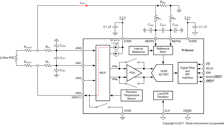
Figure 78 shows a typical circuit implementation of a 2-wire RTD measurement. The main difference compared to a 3-wire RTD measurement is with respect to the lead resistance compensation. The voltage drop across the lead resistors, RLEAD1 and RLEAD2, in this configuration is directly part of the measurement (as shown in Equation 40) because there is no means to compensate the lead resistance by use of the second current source. Any compensation must be done by calibration.
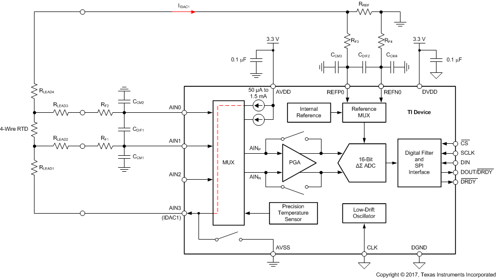
Figure 79 shows a typical circuit implementation of a 4-wire RTD measurement. Similar to the 2-wire RTD measurement, only one IDAC is required for exciting and measuring a 4-wire RTD in a ratiometric manner. The main benefit of using a 4-wire RTD is that the ADC inputs are connected to the RTD in the form of a Kelvin connection. Apart from the input leakage currents of the ADC, there is no current flow through the lead resistors RLEAD2 and RLEAD3 and therefore no voltage drop is created across them. The voltage at the ADC inputs consequently equals the voltage across the RTD and the lead resistance is of no concern.
Note that because only one IDAC is used and flows through the reference resistor, RREF, the transfer function of a 2- and 4-wire RTD measurement differs compared to the one of a 3-wire RTD measurement by a factor of 2, as shown in Equation 41.
In addition, the common-mode and reference voltage is reduced compared to the 3-wire RTD configuration. Therefore, some further modifications may be required in case the 3-wire RTD design is used to measure 2- and 4-wire RTDs as well. If the decreased common-mode voltage does not meet the VCM (MIN) requirements of the PGA anymore, either increase the value of RREF by switching in a larger resistor or, alternatively, increase the excitation current while decreasing the gain at the same time.
9.2.2.3 Application Curves
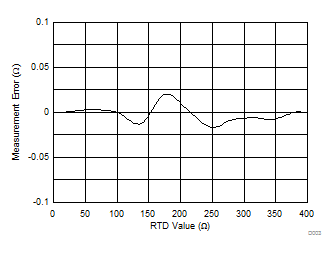
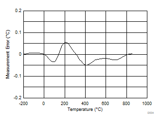
Figure 80 and Figure 81 show the measurement results. The measurements are taken at TA = 25°C. A system offset calibration is performed using a reference resistor of 100 Ω. No gain calibration is implemented. The data in Figure 80 are taken using precision resistors instead of a 3-wire Pt100. The respective temperature measurement error in Figure 81 is calculated from the data in Figure 80 using the NIST tables.
The design meets the required temperature measurement accuracy given in Table 23. Note that the measurement error shown in Figure 81 does not include the error of the RTD itself.
9.2.3 Resistive Bridge Measurement
The device offers several features to ease the implementation of ratiometric bridge measurements (such as a PGA with gains up to 128, buffered, differential reference inputs, and a low-side power switch).
9.2.3.1 Design Requirements
Table 25. Design Requirements
| DESIGN PARAMETER | VALUE |
|---|---|
| Analog supply voltage | 5.0 V |
| Digital supply voltage | 3.3 V |
| Load cell type | 4-wire load cell |
| Load cell sensitivity | 2 mV/V |
| Excitation voltage | 5 V |
| Noise-free counts | 8000 |
9.2.3.2 Detailed Design Procedure
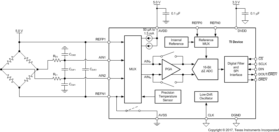
To implement a ratiometric bridge measurement, the bridge excitation voltage is simultaneously used as the reference voltage for the ADC; see Figure 82. With this configuration, any drift in excitation voltage also shows up on the reference voltage, consequently canceling out drift error. Either of the two device reference input pairs can be connected to the bridge excitation voltage. However, only the negative reference input (REFN1) can be internally routed to a low-side power switch. By connecting the low side of the bridge to REFN1, the device can automatically power-down the bridge by opening the low-side power switch. When the PSW bit in the configuration register is set to 1, the device opens the switch every time a POWERDOWN command is issued and closes the switch again when a START/SYNC command is sent.
The PGA offers gains up to 128, which helps amplify the small differential bridge output signal to make optimal use of the ADC full-scale range. Using a symmetrical bridge with the excitation voltage equal to the supply voltage of the device ensures that the output signal of the bridge meets the common-mode voltage requirement of the PGA.
Note that the maximum input voltage of ADS1120 is limited to VIN (MAX) = ±[(AVDD – AVSS) – 0.4 V] / Gain, which means the entire full-scale range, FSR = ±(AVDD – AVSS) / Gain, cannot be used in this configuration. This limitation is a result of the output drive capability of the PGA amplifiers (A1 and A2); see Figure 39. The output of each amplifier must stay 200 mV away from the rails (AVDD and AVSS), otherwise the PGA becomes nonlinear. Consequently, the maximum output swing of the PGA is limited to VOUT = ±[(AVDD – AVSS) – 0.4 V].
Using a 2-mV/V load cell with a 5-V excitation yields a maximum differential output voltage of VIN (MAX) = ±10 mV, which meets Equation 42 when using a gain of 128.
A first-order differential and common-mode RC filter (RF1, RF2, CDIF1, CCM1, and CCM2) is placed on the ADC inputs. The reference has an additional capacitor CDIF2 to limit reference noise. Care must be taken to maintain a limited amount of filtering or the measurement will no longer be ratiometric.
The device is capable of 16-bit, noise-free resolution using a gain of 128 at 20 SPS for the specified reference voltage. Accordingly the device is able to resolve signals as small as one LSB. The LSB size is calculated using Equation 43:
To find the total number of counts available for the bridge measurement, the maximum output voltage is divided by the LSB value. Dividing 10 mV by 1.192 µV equates to 8389 total counts available, which meets the design parameter of 8000 counts.
The register settings for this design are shown in Table 26.
Table 26. Register Settings
| REGISTER | SETTING | DESCRIPTION |
|---|---|---|
| 00h | 3Eh | AINP = AIN1, AINN = AIN2, gain = 128, PGA enabled |
| 01h | 04h | DR = 20 SPS, normal mode, continuous conversion mode |
| 02h | 98h | External reference (REFP1, REFN1), simultaneous 50-Hz and 60-Hz rejection, PSW = 1 |
| 03h | 00h | No IDACs used |
