ZHCSGA6A February 2017 – June 2017 ADS114S06 , ADS114S08
PRODUCTION DATA.
- 1 特性
- 2 应用
- 3 说明
- 4 修订历史记录
- 5 Device Family Comparison Table
- 6 Pin Configuration and Functions
- 7 Specifications
- 8 Parameter Measurement Information
-
9 Detailed Description
- 9.1 Overview
- 9.2 Functional Block Diagram
- 9.3
Feature Description
- 9.3.1 Multiplexer
- 9.3.2 Low-Noise Programmable Gain Amplifier
- 9.3.3 Voltage Reference
- 9.3.4 Clock Source
- 9.3.5 Delta-Sigma Modulator
- 9.3.6 Digital Filter
- 9.3.7 Excitation Current Sources (IDACs)
- 9.3.8 Bias Voltage Generation
- 9.3.9 System Monitor
- 9.3.10 Status Register
- 9.3.11 General-Purpose Inputs and Outputs (GPIOs)
- 9.3.12 Low-Side Power Switch
- 9.3.13 Cyclic Redundancy Check (CRC)
- 9.3.14 Calibration
- 9.4 Device Functional Modes
- 9.5 Programming
- 9.6
Register Map
- 9.6.1
Configuration Registers
- 9.6.1.1 Device ID Register (address = 00h) [reset = xxh]
- 9.6.1.2 Device Status Register (address = 01h) [reset = 80h]
- 9.6.1.3 Input Multiplexer Register (address = 02h) [reset = 01h]
- 9.6.1.4 Gain Setting Register (address = 03h) [reset = 00h]
- 9.6.1.5 Data Rate Register (address = 04h) [reset = 14h]
- 9.6.1.6 Reference Control Register (address = 05h) [reset = 10h]
- 9.6.1.7 Excitation Current Register 1 (address = 06h) [reset = 00h]
- 9.6.1.8 Excitation Current Register 2 (address = 07h) [reset = FFh]
- 9.6.1.9 Sensor Biasing Register (address = 08h) [reset = 00h]
- 9.6.1.10 System Control Register (address = 09h) [reset = 10h]
- 9.6.1.11 Reserved Register (address = 0Ah) [reset = 00h]
- 9.6.1.12 Offset Calibration Register 1 (address = 0Bh) [reset = 00h]
- 9.6.1.13 Offset Calibration Register 2 (address = 0Ch) [reset = 00h]
- 9.6.1.14 Reserved Register (address = 0Dh) [reset = 00h]
- 9.6.1.15 Gain Calibration Register 1 (address = 0Eh) [reset = 00h]
- 9.6.1.16 Gain Calibration Register 2 (address = 0Fh) [reset = 40h]
- 9.6.1.17 GPIO Data Register (address = 10h) [reset = 00h]
- 9.6.1.18 GPIO Configuration Register (address = 11h) [reset = 00h]
- 9.6.1
Configuration Registers
- 10Application and Implementation
- 11Power Supply Recommendations
- 12Layout
- 13器件和文档支持
- 14机械、封装和可订购信息
封装选项
机械数据 (封装 | 引脚)
散热焊盘机械数据 (封装 | 引脚)
- PBS|32
订购信息
10.2 Typical Application
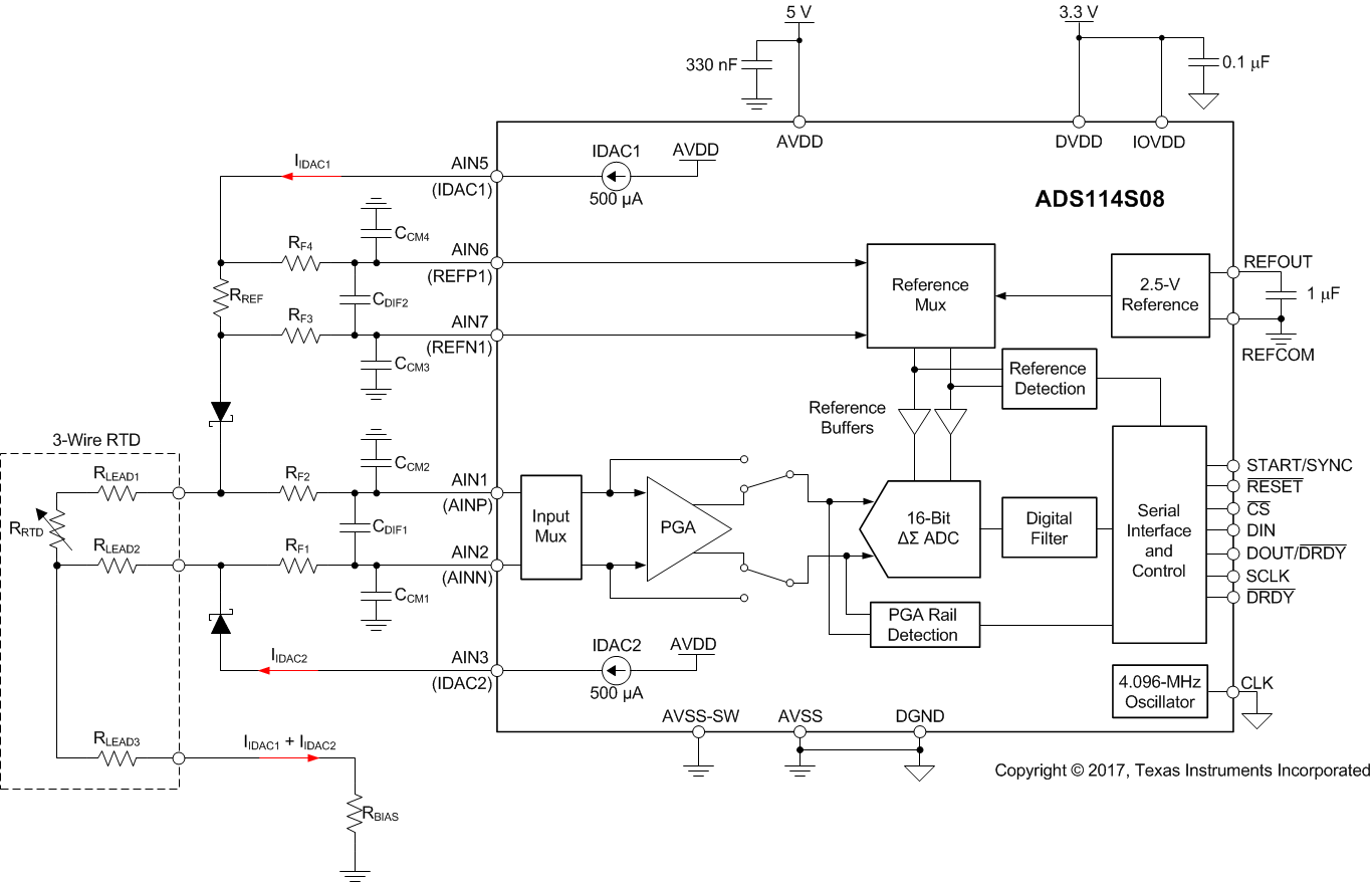
Figure 113 shows a fault-protected, filtered, 3-wire RTD application circuit with hardware-based, lead-wire compensation. Two IDAC current sources provide the lead-wire compensation. One IDAC current source (IDAC1) provides excitation to the RTD element. The ADC reference voltage (pins AIN6 and AIN7) is derived from the voltage across resistor RREF sourcing the same IDAC1 current, providing ratiometric cancellation of current-source drift. The other current source (IDAC2) has the same current setting, providing cancellation of lead-wire resistance by generating a voltage drop across lead-wire resistance RLEAD2 equal to the voltage drop of RLEAD1. Because the RRTD voltage is measured differentially at ADC pins AIN1 and AIN2, the voltages across the lead wire resistance cancel. Resistor RBIAS level-shifts the RTD signal to within the ADC specified input range. The current sources are provided by two additional pins (AIN5 and AIN3) that connect to the RTD through blocking diodes. The additional pins are used to route the RTD excitation currents around the input filter resistors, avoiding the voltage drop otherwise caused by the filter resistors RF1 and RF4. The diodes protect the ADC inputs in the event of a miswired connection. The input filter resistors limit the input fault currents flowing into the ADC.
 Figure 113. 3-Wire RTD Application