ZHCSGA6A February 2017 – June 2017 ADS114S06 , ADS114S08
PRODUCTION DATA.
- 1 特性
- 2 应用
- 3 说明
- 4 修订历史记录
- 5 Device Family Comparison Table
- 6 Pin Configuration and Functions
- 7 Specifications
- 8 Parameter Measurement Information
-
9 Detailed Description
- 9.1 Overview
- 9.2 Functional Block Diagram
- 9.3
Feature Description
- 9.3.1 Multiplexer
- 9.3.2 Low-Noise Programmable Gain Amplifier
- 9.3.3 Voltage Reference
- 9.3.4 Clock Source
- 9.3.5 Delta-Sigma Modulator
- 9.3.6 Digital Filter
- 9.3.7 Excitation Current Sources (IDACs)
- 9.3.8 Bias Voltage Generation
- 9.3.9 System Monitor
- 9.3.10 Status Register
- 9.3.11 General-Purpose Inputs and Outputs (GPIOs)
- 9.3.12 Low-Side Power Switch
- 9.3.13 Cyclic Redundancy Check (CRC)
- 9.3.14 Calibration
- 9.4 Device Functional Modes
- 9.5 Programming
- 9.6
Register Map
- 9.6.1
Configuration Registers
- 9.6.1.1 Device ID Register (address = 00h) [reset = xxh]
- 9.6.1.2 Device Status Register (address = 01h) [reset = 80h]
- 9.6.1.3 Input Multiplexer Register (address = 02h) [reset = 01h]
- 9.6.1.4 Gain Setting Register (address = 03h) [reset = 00h]
- 9.6.1.5 Data Rate Register (address = 04h) [reset = 14h]
- 9.6.1.6 Reference Control Register (address = 05h) [reset = 10h]
- 9.6.1.7 Excitation Current Register 1 (address = 06h) [reset = 00h]
- 9.6.1.8 Excitation Current Register 2 (address = 07h) [reset = FFh]
- 9.6.1.9 Sensor Biasing Register (address = 08h) [reset = 00h]
- 9.6.1.10 System Control Register (address = 09h) [reset = 10h]
- 9.6.1.11 Reserved Register (address = 0Ah) [reset = 00h]
- 9.6.1.12 Offset Calibration Register 1 (address = 0Bh) [reset = 00h]
- 9.6.1.13 Offset Calibration Register 2 (address = 0Ch) [reset = 00h]
- 9.6.1.14 Reserved Register (address = 0Dh) [reset = 00h]
- 9.6.1.15 Gain Calibration Register 1 (address = 0Eh) [reset = 00h]
- 9.6.1.16 Gain Calibration Register 2 (address = 0Fh) [reset = 40h]
- 9.6.1.17 GPIO Data Register (address = 10h) [reset = 00h]
- 9.6.1.18 GPIO Configuration Register (address = 11h) [reset = 00h]
- 9.6.1
Configuration Registers
- 10Application and Implementation
- 11Power Supply Recommendations
- 12Layout
- 13器件和文档支持
- 14机械、封装和可订购信息
封装选项
机械数据 (封装 | 引脚)
散热焊盘机械数据 (封装 | 引脚)
- PBS|32
订购信息
9.3.2.1 PGA Input-Voltage Requirements
As with many amplifiers, the PGA has an absolute input voltage range requirement that cannot be exceeded. The maximum and minimum absolute input voltages are limited by the voltage swing capability of the PGA output. The specified minimum and maximum absolute input voltages (VAINP and VAINN) depend on the PGA gain, the maximum differential input voltage (VINMAX), and the tolerance of the analog power-supply voltages (AVDD and AVSS). Use the maximum voltage expected in the application for VINMAX. The absolute positive and negative input voltages must be within the specified range, as shown in Equation 5:
where
- VAINP, VAINN = absolute input voltage
- VINMAX = VAINP – VAINN = maximum differential input voltage
As mentioned in the previous section, PGA gain settings of 64 and 128 are scaled in the digital domain and are not implemented with the amplifier. When using the PGA in gains of 64 and 128, set the gain in Equation 5 to 32 to calculate the absolute input voltage range.
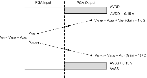
The relationship between the PGA input to the PGA output is shown graphically in Figure 51. The PGA output voltages (VOUTP, VOUTN) depend on the PGA gain and the input voltage magnitudes. For linear operation, the PGA output voltages must not exceed AVDD – 0.15 V or AVSS + 0.15 V. Note that the diagram depicts a positive differential input voltage that results in a positive differential output voltage.
 Figure 51. PGA Input/Output Range
Download the ADS1x4S0x design calculator from www.ti.com. This calculator can be used to determine the input voltage range of the PGA.