ZHCSGA6A February 2017 – June 2017 ADS114S06 , ADS114S08
PRODUCTION DATA.
- 1 特性
- 2 应用
- 3 说明
- 4 修订历史记录
- 5 Device Family Comparison Table
- 6 Pin Configuration and Functions
- 7 Specifications
- 8 Parameter Measurement Information
-
9 Detailed Description
- 9.1 Overview
- 9.2 Functional Block Diagram
- 9.3
Feature Description
- 9.3.1 Multiplexer
- 9.3.2 Low-Noise Programmable Gain Amplifier
- 9.3.3 Voltage Reference
- 9.3.4 Clock Source
- 9.3.5 Delta-Sigma Modulator
- 9.3.6 Digital Filter
- 9.3.7 Excitation Current Sources (IDACs)
- 9.3.8 Bias Voltage Generation
- 9.3.9 System Monitor
- 9.3.10 Status Register
- 9.3.11 General-Purpose Inputs and Outputs (GPIOs)
- 9.3.12 Low-Side Power Switch
- 9.3.13 Cyclic Redundancy Check (CRC)
- 9.3.14 Calibration
- 9.4 Device Functional Modes
- 9.5 Programming
- 9.6
Register Map
- 9.6.1
Configuration Registers
- 9.6.1.1 Device ID Register (address = 00h) [reset = xxh]
- 9.6.1.2 Device Status Register (address = 01h) [reset = 80h]
- 9.6.1.3 Input Multiplexer Register (address = 02h) [reset = 01h]
- 9.6.1.4 Gain Setting Register (address = 03h) [reset = 00h]
- 9.6.1.5 Data Rate Register (address = 04h) [reset = 14h]
- 9.6.1.6 Reference Control Register (address = 05h) [reset = 10h]
- 9.6.1.7 Excitation Current Register 1 (address = 06h) [reset = 00h]
- 9.6.1.8 Excitation Current Register 2 (address = 07h) [reset = FFh]
- 9.6.1.9 Sensor Biasing Register (address = 08h) [reset = 00h]
- 9.6.1.10 System Control Register (address = 09h) [reset = 10h]
- 9.6.1.11 Reserved Register (address = 0Ah) [reset = 00h]
- 9.6.1.12 Offset Calibration Register 1 (address = 0Bh) [reset = 00h]
- 9.6.1.13 Offset Calibration Register 2 (address = 0Ch) [reset = 00h]
- 9.6.1.14 Reserved Register (address = 0Dh) [reset = 00h]
- 9.6.1.15 Gain Calibration Register 1 (address = 0Eh) [reset = 00h]
- 9.6.1.16 Gain Calibration Register 2 (address = 0Fh) [reset = 40h]
- 9.6.1.17 GPIO Data Register (address = 10h) [reset = 00h]
- 9.6.1.18 GPIO Configuration Register (address = 11h) [reset = 00h]
- 9.6.1
Configuration Registers
- 10Application and Implementation
- 11Power Supply Recommendations
- 12Layout
- 13器件和文档支持
- 14机械、封装和可订购信息
封装选项
机械数据 (封装 | 引脚)
散热焊盘机械数据 (封装 | 引脚)
- PBS|32
订购信息
9.3.8 Bias Voltage Generation
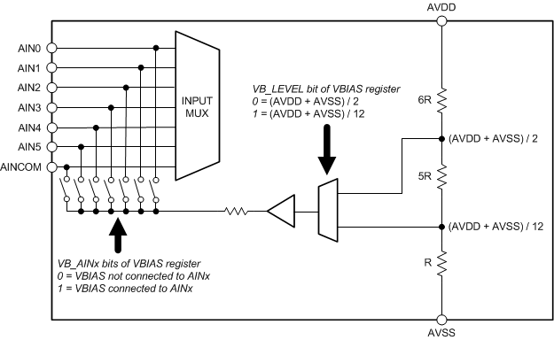
The ADS114S0x provides an internal bias voltage generator, VBIAS, that can be set to two different levels,
(AVDD + AVSS) / 2 and (AVDD + AVSS) / 12 by using the VB_LEVEL bit in the sensor biasing register (08h). The bias voltage is internally buffered and can be established on the analog inputs AIN0 to AIN5 and AINCOM using the VB_AINx bits in the sensor biasing register (08h). A typical use case for VBIAS is biasing unbiased thermocouples to within the common-mode voltage range of the PGA. A block diagram of the VBIAS voltage generator and connection diagram is shown in Figure 76.
 Figure 76. VBIAS Block Diagram
The start-up time of the VBIAS voltage depends on the pin load capacitance. The total capacitance includes any capacitance connected from VBIAS to AVDD, AVSS, and ground. Table 20 lists the VBIAS voltage settling times for various external load capacitances. Ensure the VBIAS voltage is fully settled before starting a conversion.
Table 20. VBIAS Settling Time
| LOAD CAPACITANCE | SETTLING TIME |
|---|---|
| 0.1 µF | 280 µs |
| 1 µF | 2.8 ms |
| 10 µF | 28 ms |