ZHCSGS4A August   2017  – February 2020 ADS114S06B , ADS114S08B

PRODUCTION DATA.  

  1. 特性
  2. 应用
  3. 说明
    1.     Device Images
      1.      功能方框图
  4. 修订历史记录
  5. Device Comparison Table
  6. Pin Configuration and Functions
    1.     Pin Functions
  7. Specifications
    1. 7.1 Absolute Maximum Ratings
    2. 7.2 ESD Ratings
    3. 7.3 Recommended Operating Conditions
    4. 7.4 Thermal Information
    5. 7.5 Electrical Characteristics
    6. 7.6 Timing Requirements
    7. 7.7 Switching Characteristics
    8. 7.8 Typical Characteristics
  8. Parameter Measurement Information
    1. 8.1 Noise Performance
  9. Detailed Description
    1. 9.1 Overview
    2. 9.2 Functional Block Diagram
    3. 9.3 Feature Description
      1. 9.3.1  Multiplexer
      2. 9.3.2  Low-Noise Programmable Gain Amplifier
        1. 9.3.2.1 PGA Input-Voltage Requirements
        2. 9.3.2.2 Bypassing the PGA
      3. 9.3.3  Voltage Reference
        1. 9.3.3.1 Internal Reference
        2. 9.3.3.2 External Reference
        3. 9.3.3.3 Reference Buffers
      4. 9.3.4  Clock Source
      5. 9.3.5  Delta-Sigma Modulator
      6. 9.3.6  Digital Filter
        1. 9.3.6.1 Digital Filter Frequency Response
        2. 9.3.6.2 Data Conversion Time
        3. 9.3.6.3 Note on Conversion Time
        4. 9.3.6.4 50-Hz and 60-Hz Line Cycle Rejection
      7. 9.3.7  Excitation Current Sources (IDACs)
      8. 9.3.8  Bias Voltage Generation
      9. 9.3.9  System Monitor
        1. 9.3.9.1 Internal Temperature Sensor
        2. 9.3.9.2 Power Supply Monitors
        3. 9.3.9.3 Burn-Out Current Sources
      10. 9.3.10 Status Register
        1. 9.3.10.1 POR Flag
        2. 9.3.10.2 RDY Flag
        3. 9.3.10.3 External Reference Monitor
      11. 9.3.11 General-Purpose Inputs and Outputs (GPIOs)
      12. 9.3.12 Calibration
        1. 9.3.12.1 Offset Calibration
        2. 9.3.12.2 Gain Calibration
    4. 9.4 Device Functional Modes
      1. 9.4.1 Reset
        1. 9.4.1.1 Power-On Reset
        2. 9.4.1.2 RESET Pin
        3. 9.4.1.3 Reset by Command
      2. 9.4.2 Power-Down Mode
      3. 9.4.3 Standby Mode
      4. 9.4.4 Conversion Modes
        1. 9.4.4.1 Continuous Conversion Mode
        2. 9.4.4.2 Single-Shot Conversion Mode
    5. 9.5 Programming
      1. 9.5.1 Serial Interface
        1. 9.5.1.1 Chip Select (CS)
        2. 9.5.1.2 Serial Clock (SCLK)
        3. 9.5.1.3 Serial Data Input (DIN)
        4. 9.5.1.4 Serial Data Output and Data Ready (DOUT/DRDY)
        5. 9.5.1.5 Data Ready (DRDY)
        6. 9.5.1.6 Timeout
      2. 9.5.2 Data Format
      3. 9.5.3 Commands
        1. 9.5.3.1  NOP
        2. 9.5.3.2  WAKEUP
        3. 9.5.3.3  POWERDOWN
        4. 9.5.3.4  RESET
        5. 9.5.3.5  START
        6. 9.5.3.6  STOP
        7. 9.5.3.7  SYOCAL
        8. 9.5.3.8  SYGCAL
        9. 9.5.3.9  SFOCAL
        10. 9.5.3.10 RDATA
        11. 9.5.3.11 RREG
        12. 9.5.3.12 WREG
      4. 9.5.4 Interfacing with Multiple Devices
    6. 9.6 Register Map
      1. 9.6.1 Configuration Registers
      2. 9.6.2 Register Descriptions
        1. 9.6.2.1  Device ID Register (address = 00h) [reset = xxh]
          1. Table 16. Device ID (ID) Register Field Descriptions
        2. 9.6.2.2  Device Status Register (address = 01h) [reset = 80h]
          1. Table 17. Device Status (STATUS) Register Field Descriptions
        3. 9.6.2.3  Input Multiplexer Register (address = 02h) [reset = 01h]
          1. Table 18. Input Multiplexer (INPMUX) Register Field Descriptions
        4. 9.6.2.4  Gain Setting Register (address = 03h) [reset = 00h]
          1. Table 19. Gain Setting (PGA) Register Field Descriptions
        5. 9.6.2.5  Data Rate Register (address = 04h) [reset = 14h]
          1. Table 20. Data Rate (DATARATE) Register Field Descriptions
        6. 9.6.2.6  Reference Control Register (address = 05h) [reset = 10h]
          1. Table 21. Reference Control (REF) Register Field Descriptions
        7. 9.6.2.7  Excitation Current Register 1 (address = 06h) [reset = 00h]
          1. Table 22. Excitation Current Register 1 (IDACMAG) Register Field Descriptions
        8. 9.6.2.8  Excitation Current Register 2 (address = 07h) [reset = FFh]
          1. Table 23. Excitation Current Register 2 (IDACMUX) Register Field Descriptions
        9. 9.6.2.9  Sensor Biasing Register (address = 08h) [reset = 00h]
          1. Table 24. Sensor Biasing (VBIAS) Register Field Descriptions
        10. 9.6.2.10 System Control Register (address = 09h) [reset = 10h]
          1. Table 25. System Control (SYS) Register Field Descriptions
        11. 9.6.2.11 Reserved Register (address = 0Ah) [reset = 00h]
          1. Table 26. Reserved Register Field Descriptions
        12. 9.6.2.12 Offset Calibration Register 1 (address = 0Bh) [reset = 00h]
          1. Table 27. Offset Calibration Register 1 (OFCAL0) Register Field Descriptions
        13. 9.6.2.13 Offset Calibration Register 2 (address = 0Ch) [reset = 00h]
          1. Table 28. Offset Calibration Register 2 (OFCAL1) Register Field Descriptions
        14. 9.6.2.14 Reserved Register (address = 0Dh) [reset = 00h]
          1. Table 29. Reserved Register Field Descriptions
        15. 9.6.2.15 Gain Calibration Register 1 (address = 0Eh) [reset = 00h]
          1. Table 30. Gain Calibration Register 1 (FSCAL0) Field Descriptions
        16. 9.6.2.16 Gain Calibration Register 2 (address = 0Fh) [reset = 40h]
          1. Table 31. Gain Calibration Register 2 (FSCAL1) Field Descriptions
        17. 9.6.2.17 GPIO Data Register (address = 10h) [reset = 00h]
          1. Table 32. GPIO Data (GPIODAT) Register Field Descriptions
        18. 9.6.2.18 GPIO Configuration Register (address = 11h) [reset = 00h]
          1. Table 33. GPIO Configuration (GPIOCON) Register Field Descriptions
  10. 10Application and Implementation
    1. 10.1 Application Information
      1. 10.1.1 Serial Interface Connections
      2. 10.1.2 Analog Input Filtering
      3. 10.1.3 External Reference and Ratiometric Measurements
      4. 10.1.4 Establishing a Proper Input Voltage
      5. 10.1.5 Unused Inputs and Outputs
      6. 10.1.6 Pseudo Code Example
    2. 10.2 Typical Application
      1. 10.2.1 Design Requirements
      2. 10.2.2 Detailed Design Procedure
        1. 10.2.2.1 Register Settings
      3. 10.2.3 Application Curves
    3. 10.3 What To Do and What Not To Do
  11. 11Power Supply Recommendations
    1. 11.1 Power Supplies
    2. 11.2 Power-Supply Sequencing
    3. 11.3 Power-On Reset
    4. 11.4 Power-Supply Decoupling
  12. 12Layout
    1. 12.1 Layout Guidelines
    2. 12.2 Layout Example
  13. 13器件和文档支持
    1. 13.1 器件支持
      1. 13.1.1 开发支持
    2. 13.2 文档支持
      1. 13.2.1 相关文档
    3. 13.3 相关链接
    4. 13.4 接收文档更新通知
    5. 13.5 社区资源
    6. 13.6 商标
    7. 13.7 静电放电警告
    8. 13.8 Glossary
  14. 14机械、封装和可订购信息

封装选项

请参考 PDF 数据表获取器件具体的封装图。

机械数据 (封装 | 引脚)
  • RHB|32
  • PBS|32
散热焊盘机械数据 (封装 | 引脚)
订购信息

Bias Voltage Generation

The ADS114S0xB provides an internal bias voltage generator, VBIAS, that is set to (AVDD + AVSS) / 2. The bias voltage is internally buffered and can be established on the analog inputs AIN0 to AIN5 and AINCOM using the VB_AINx bits in the sensor biasing register (08h). A typical use case for VBIAS is biasing unbiased thermocouples to within the common-mode voltage range of the PGA. Figure 64 shows a block diagram of the VBIAS voltage generator and connection diagram.
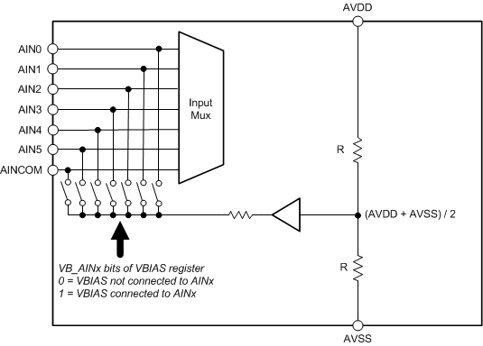
ADS114S06B ADS114S08B ai_vbias_mux_sbas852.gifFigure 64. VBIAS Block Diagram

The start-up time of the VBIAS voltage depends on the pin load capacitance. The total capacitance includes any capacitance connected from VBIAS to AVDD, AVSS, and ground. Table 9 lists the VBIAS voltage settling times for various external load capacitances. Ensure the VBIAS voltage is fully settled before starting a conversion.

Table 9. VBIAS Settling Time

LOAD CAPACITANCE SETTLING TIME
0.1 µF 280 µs
1 µF 2.8 ms
10 µF 28 ms