ZHCSGS4A August 2017 – February 2020 ADS114S06B , ADS114S08B
PRODUCTION DATA.
- 1 特性
- 2 应用
- 3 说明
- 4 修订历史记录
- 5 Device Comparison Table
- 6 Pin Configuration and Functions
- 7 Specifications
- 8 Parameter Measurement Information
-
9 Detailed Description
- 9.1 Overview
- 9.2 Functional Block Diagram
- 9.3
Feature Description
- 9.3.1 Multiplexer
- 9.3.2 Low-Noise Programmable Gain Amplifier
- 9.3.3 Voltage Reference
- 9.3.4 Clock Source
- 9.3.5 Delta-Sigma Modulator
- 9.3.6 Digital Filter
- 9.3.7 Excitation Current Sources (IDACs)
- 9.3.8 Bias Voltage Generation
- 9.3.9 System Monitor
- 9.3.10 Status Register
- 9.3.11 General-Purpose Inputs and Outputs (GPIOs)
- 9.3.12 Calibration
- 9.4 Device Functional Modes
- 9.5 Programming
- 9.6
Register Map
- 9.6.1 Configuration Registers
- 9.6.2
Register Descriptions
- 9.6.2.1 Device ID Register (address = 00h) [reset = xxh]
- 9.6.2.2 Device Status Register (address = 01h) [reset = 80h]
- 9.6.2.3 Input Multiplexer Register (address = 02h) [reset = 01h]
- 9.6.2.4 Gain Setting Register (address = 03h) [reset = 00h]
- 9.6.2.5 Data Rate Register (address = 04h) [reset = 14h]
- 9.6.2.6 Reference Control Register (address = 05h) [reset = 10h]
- 9.6.2.7 Excitation Current Register 1 (address = 06h) [reset = 00h]
- 9.6.2.8 Excitation Current Register 2 (address = 07h) [reset = FFh]
- 9.6.2.9 Sensor Biasing Register (address = 08h) [reset = 00h]
- 9.6.2.10 System Control Register (address = 09h) [reset = 10h]
- 9.6.2.11 Reserved Register (address = 0Ah) [reset = 00h]
- 9.6.2.12 Offset Calibration Register 1 (address = 0Bh) [reset = 00h]
- 9.6.2.13 Offset Calibration Register 2 (address = 0Ch) [reset = 00h]
- 9.6.2.14 Reserved Register (address = 0Dh) [reset = 00h]
- 9.6.2.15 Gain Calibration Register 1 (address = 0Eh) [reset = 00h]
- 9.6.2.16 Gain Calibration Register 2 (address = 0Fh) [reset = 40h]
- 9.6.2.17 GPIO Data Register (address = 10h) [reset = 00h]
- 9.6.2.18 GPIO Configuration Register (address = 11h) [reset = 00h]
- 10Application and Implementation
- 11Power Supply Recommendations
- 12Layout
- 13器件和文档支持
- 14机械、封装和可订购信息
封装选项
请参考 PDF 数据表获取器件具体的封装图。
机械数据 (封装 | 引脚)
- RHB|32
- PBS|32
散热焊盘机械数据 (封装 | 引脚)
- PBS|32
订购信息
9.3.11 General-Purpose Inputs and Outputs (GPIOs)
The ADS114S06B offers four dedicated general-purpose input and output (GPIO) pins, and the ADS114S08B offers four pins (AIN8 to AIN11) that serve a dual purpose as either analog inputs or GPIOs.
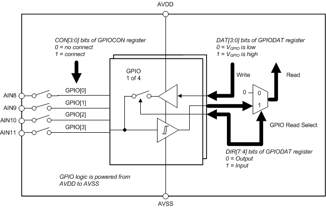
Two registers control the function of the GPIO pins. Use the CON[3:0] bits of the GPIO configuration register (11h) to configure a pin as a GPIO pin. The upper four bits (DIR[3:0]) of the GPIO data register (10h) configure the GPIO pin as either an input or an output. The lower four bits (DAT[3:0]) of the GPIO data register contain the input or output GPIO data. If a GPIO pin is configured as an input, the respective DAT[x] bit reads the status of the pin; if a GPIO pin is configured as an output, write the output status to the respective DAT[x] bit. For more information about the use of GPIO pins, see the Configuration Registers section.
Figure 65 depicts a diagram of how these functions are combined onto a single pin. When the pin is configured as a GPIO, the corresponding logic is powered from AVDD and AVSS. When the devices are operated with bipolar analog supplies, the GPIO outputs bipolar voltages. Care must be taken to not load the GPIO pins when used as outputs because large currents can cause droop or noise on the analog supplies. GPIO pins use Schmitt triggered inputs with hysteresis to make the input more resistance to noise; see the Electrical Characteristics table for GPIO thresholds.
For connections of unused GPIO pins, see the Unused Inputs and Outputs section.
 Figure 65. GPIO Block Diagram