ZHCSGS4A August 2017 – February 2020 ADS114S06B , ADS114S08B
PRODUCTION DATA.
- 1 特性
- 2 应用
- 3 说明
- 4 修订历史记录
- 5 Device Comparison Table
- 6 Pin Configuration and Functions
- 7 Specifications
- 8 Parameter Measurement Information
-
9 Detailed Description
- 9.1 Overview
- 9.2 Functional Block Diagram
- 9.3
Feature Description
- 9.3.1 Multiplexer
- 9.3.2 Low-Noise Programmable Gain Amplifier
- 9.3.3 Voltage Reference
- 9.3.4 Clock Source
- 9.3.5 Delta-Sigma Modulator
- 9.3.6 Digital Filter
- 9.3.7 Excitation Current Sources (IDACs)
- 9.3.8 Bias Voltage Generation
- 9.3.9 System Monitor
- 9.3.10 Status Register
- 9.3.11 General-Purpose Inputs and Outputs (GPIOs)
- 9.3.12 Calibration
- 9.4 Device Functional Modes
- 9.5 Programming
- 9.6
Register Map
- 9.6.1 Configuration Registers
- 9.6.2
Register Descriptions
- 9.6.2.1 Device ID Register (address = 00h) [reset = xxh]
- 9.6.2.2 Device Status Register (address = 01h) [reset = 80h]
- 9.6.2.3 Input Multiplexer Register (address = 02h) [reset = 01h]
- 9.6.2.4 Gain Setting Register (address = 03h) [reset = 00h]
- 9.6.2.5 Data Rate Register (address = 04h) [reset = 14h]
- 9.6.2.6 Reference Control Register (address = 05h) [reset = 10h]
- 9.6.2.7 Excitation Current Register 1 (address = 06h) [reset = 00h]
- 9.6.2.8 Excitation Current Register 2 (address = 07h) [reset = FFh]
- 9.6.2.9 Sensor Biasing Register (address = 08h) [reset = 00h]
- 9.6.2.10 System Control Register (address = 09h) [reset = 10h]
- 9.6.2.11 Reserved Register (address = 0Ah) [reset = 00h]
- 9.6.2.12 Offset Calibration Register 1 (address = 0Bh) [reset = 00h]
- 9.6.2.13 Offset Calibration Register 2 (address = 0Ch) [reset = 00h]
- 9.6.2.14 Reserved Register (address = 0Dh) [reset = 00h]
- 9.6.2.15 Gain Calibration Register 1 (address = 0Eh) [reset = 00h]
- 9.6.2.16 Gain Calibration Register 2 (address = 0Fh) [reset = 40h]
- 9.6.2.17 GPIO Data Register (address = 10h) [reset = 00h]
- 9.6.2.18 GPIO Configuration Register (address = 11h) [reset = 00h]
- 10Application and Implementation
- 11Power Supply Recommendations
- 12Layout
- 13器件和文档支持
- 14机械、封装和可订购信息
封装选项
请参考 PDF 数据表获取器件具体的封装图。
机械数据 (封装 | 引脚)
- RHB|32
- PBS|32
散热焊盘机械数据 (封装 | 引脚)
- PBS|32
订购信息
10.3 What To Do and What Not To Do
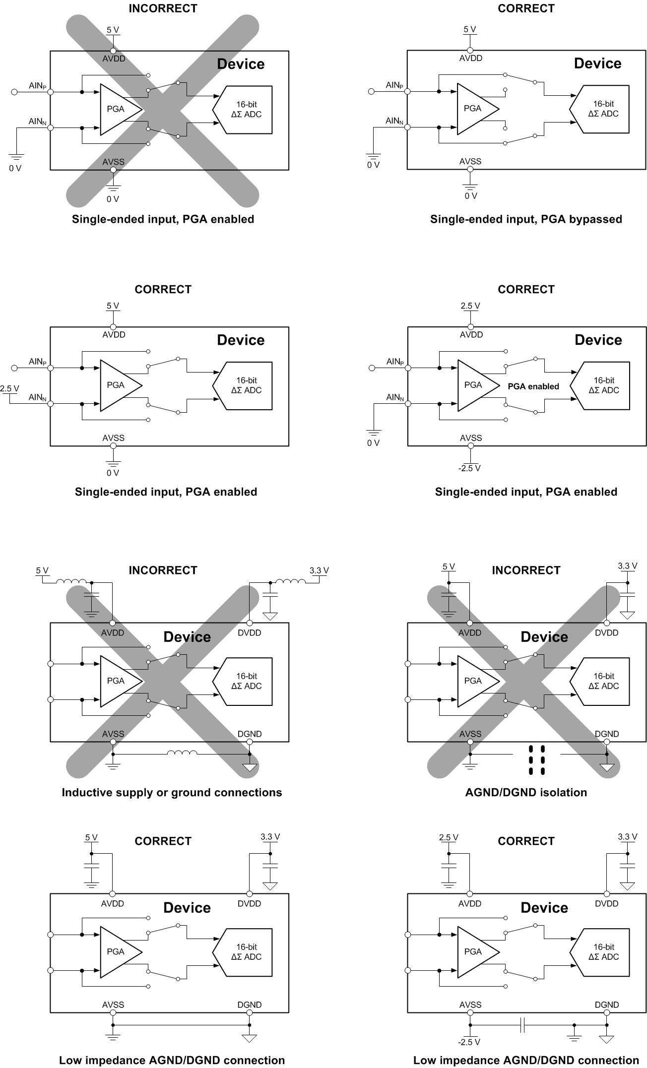
- Do partition the analog, digital, and power-supply circuitry into separate sections on the PCB.
- Do use a single ground plane for analog and digital grounds.
- Do place the analog components close to the ADC pins using short, direct connections.
- Do keep the SCLK pin free of glitches and noise.
- Do verify that the analog input voltages are within the specified PGA input voltage range under all input conditions.
- Do float unused analog input pins to minimize input leakage current on all other analog inputs. Connecting unused pins to AVDD is the next best option.
- Do provide current limiting to the analog inputs in case overvoltage faults occur.
- Do use a low-dropout linear regulator (LDO) to reduce ripple voltage generated by switch-mode power supplies. Reducing ripple is especially important for AVDD where the supply noise can affect the performance.
- Don't cross analog and digital signals.
- Don't allow the analog and digital power supply voltages to exceed 5.5 V under any condition, including during power-up and power-down.
Figure 100 shows the do's and don'ts of the ADC circuit connections.
 Figure 100. Do's and Don'ts Circuit Connections