ZHCSGS4A August   2017  – February 2020 ADS114S06B , ADS114S08B

PRODUCTION DATA.  

  1. 特性
  2. 应用
  3. 说明
    1.     Device Images
      1.      功能方框图
  4. 修订历史记录
  5. Device Comparison Table
  6. Pin Configuration and Functions
    1.     Pin Functions
  7. Specifications
    1. 7.1 Absolute Maximum Ratings
    2. 7.2 ESD Ratings
    3. 7.3 Recommended Operating Conditions
    4. 7.4 Thermal Information
    5. 7.5 Electrical Characteristics
    6. 7.6 Timing Requirements
    7. 7.7 Switching Characteristics
    8. 7.8 Typical Characteristics
  8. Parameter Measurement Information
    1. 8.1 Noise Performance
  9. Detailed Description
    1. 9.1 Overview
    2. 9.2 Functional Block Diagram
    3. 9.3 Feature Description
      1. 9.3.1  Multiplexer
      2. 9.3.2  Low-Noise Programmable Gain Amplifier
        1. 9.3.2.1 PGA Input-Voltage Requirements
        2. 9.3.2.2 Bypassing the PGA
      3. 9.3.3  Voltage Reference
        1. 9.3.3.1 Internal Reference
        2. 9.3.3.2 External Reference
        3. 9.3.3.3 Reference Buffers
      4. 9.3.4  Clock Source
      5. 9.3.5  Delta-Sigma Modulator
      6. 9.3.6  Digital Filter
        1. 9.3.6.1 Digital Filter Frequency Response
        2. 9.3.6.2 Data Conversion Time
        3. 9.3.6.3 Note on Conversion Time
        4. 9.3.6.4 50-Hz and 60-Hz Line Cycle Rejection
      7. 9.3.7  Excitation Current Sources (IDACs)
      8. 9.3.8  Bias Voltage Generation
      9. 9.3.9  System Monitor
        1. 9.3.9.1 Internal Temperature Sensor
        2. 9.3.9.2 Power Supply Monitors
        3. 9.3.9.3 Burn-Out Current Sources
      10. 9.3.10 Status Register
        1. 9.3.10.1 POR Flag
        2. 9.3.10.2 RDY Flag
        3. 9.3.10.3 External Reference Monitor
      11. 9.3.11 General-Purpose Inputs and Outputs (GPIOs)
      12. 9.3.12 Calibration
        1. 9.3.12.1 Offset Calibration
        2. 9.3.12.2 Gain Calibration
    4. 9.4 Device Functional Modes
      1. 9.4.1 Reset
        1. 9.4.1.1 Power-On Reset
        2. 9.4.1.2 RESET Pin
        3. 9.4.1.3 Reset by Command
      2. 9.4.2 Power-Down Mode
      3. 9.4.3 Standby Mode
      4. 9.4.4 Conversion Modes
        1. 9.4.4.1 Continuous Conversion Mode
        2. 9.4.4.2 Single-Shot Conversion Mode
    5. 9.5 Programming
      1. 9.5.1 Serial Interface
        1. 9.5.1.1 Chip Select (CS)
        2. 9.5.1.2 Serial Clock (SCLK)
        3. 9.5.1.3 Serial Data Input (DIN)
        4. 9.5.1.4 Serial Data Output and Data Ready (DOUT/DRDY)
        5. 9.5.1.5 Data Ready (DRDY)
        6. 9.5.1.6 Timeout
      2. 9.5.2 Data Format
      3. 9.5.3 Commands
        1. 9.5.3.1  NOP
        2. 9.5.3.2  WAKEUP
        3. 9.5.3.3  POWERDOWN
        4. 9.5.3.4  RESET
        5. 9.5.3.5  START
        6. 9.5.3.6  STOP
        7. 9.5.3.7  SYOCAL
        8. 9.5.3.8  SYGCAL
        9. 9.5.3.9  SFOCAL
        10. 9.5.3.10 RDATA
        11. 9.5.3.11 RREG
        12. 9.5.3.12 WREG
      4. 9.5.4 Interfacing with Multiple Devices
    6. 9.6 Register Map
      1. 9.6.1 Configuration Registers
      2. 9.6.2 Register Descriptions
        1. 9.6.2.1  Device ID Register (address = 00h) [reset = xxh]
          1. Table 16. Device ID (ID) Register Field Descriptions
        2. 9.6.2.2  Device Status Register (address = 01h) [reset = 80h]
          1. Table 17. Device Status (STATUS) Register Field Descriptions
        3. 9.6.2.3  Input Multiplexer Register (address = 02h) [reset = 01h]
          1. Table 18. Input Multiplexer (INPMUX) Register Field Descriptions
        4. 9.6.2.4  Gain Setting Register (address = 03h) [reset = 00h]
          1. Table 19. Gain Setting (PGA) Register Field Descriptions
        5. 9.6.2.5  Data Rate Register (address = 04h) [reset = 14h]
          1. Table 20. Data Rate (DATARATE) Register Field Descriptions
        6. 9.6.2.6  Reference Control Register (address = 05h) [reset = 10h]
          1. Table 21. Reference Control (REF) Register Field Descriptions
        7. 9.6.2.7  Excitation Current Register 1 (address = 06h) [reset = 00h]
          1. Table 22. Excitation Current Register 1 (IDACMAG) Register Field Descriptions
        8. 9.6.2.8  Excitation Current Register 2 (address = 07h) [reset = FFh]
          1. Table 23. Excitation Current Register 2 (IDACMUX) Register Field Descriptions
        9. 9.6.2.9  Sensor Biasing Register (address = 08h) [reset = 00h]
          1. Table 24. Sensor Biasing (VBIAS) Register Field Descriptions
        10. 9.6.2.10 System Control Register (address = 09h) [reset = 10h]
          1. Table 25. System Control (SYS) Register Field Descriptions
        11. 9.6.2.11 Reserved Register (address = 0Ah) [reset = 00h]
          1. Table 26. Reserved Register Field Descriptions
        12. 9.6.2.12 Offset Calibration Register 1 (address = 0Bh) [reset = 00h]
          1. Table 27. Offset Calibration Register 1 (OFCAL0) Register Field Descriptions
        13. 9.6.2.13 Offset Calibration Register 2 (address = 0Ch) [reset = 00h]
          1. Table 28. Offset Calibration Register 2 (OFCAL1) Register Field Descriptions
        14. 9.6.2.14 Reserved Register (address = 0Dh) [reset = 00h]
          1. Table 29. Reserved Register Field Descriptions
        15. 9.6.2.15 Gain Calibration Register 1 (address = 0Eh) [reset = 00h]
          1. Table 30. Gain Calibration Register 1 (FSCAL0) Field Descriptions
        16. 9.6.2.16 Gain Calibration Register 2 (address = 0Fh) [reset = 40h]
          1. Table 31. Gain Calibration Register 2 (FSCAL1) Field Descriptions
        17. 9.6.2.17 GPIO Data Register (address = 10h) [reset = 00h]
          1. Table 32. GPIO Data (GPIODAT) Register Field Descriptions
        18. 9.6.2.18 GPIO Configuration Register (address = 11h) [reset = 00h]
          1. Table 33. GPIO Configuration (GPIOCON) Register Field Descriptions
  10. 10Application and Implementation
    1. 10.1 Application Information
      1. 10.1.1 Serial Interface Connections
      2. 10.1.2 Analog Input Filtering
      3. 10.1.3 External Reference and Ratiometric Measurements
      4. 10.1.4 Establishing a Proper Input Voltage
      5. 10.1.5 Unused Inputs and Outputs
      6. 10.1.6 Pseudo Code Example
    2. 10.2 Typical Application
      1. 10.2.1 Design Requirements
      2. 10.2.2 Detailed Design Procedure
        1. 10.2.2.1 Register Settings
      3. 10.2.3 Application Curves
    3. 10.3 What To Do and What Not To Do
  11. 11Power Supply Recommendations
    1. 11.1 Power Supplies
    2. 11.2 Power-Supply Sequencing
    3. 11.3 Power-On Reset
    4. 11.4 Power-Supply Decoupling
  12. 12Layout
    1. 12.1 Layout Guidelines
    2. 12.2 Layout Example
  13. 13器件和文档支持
    1. 13.1 器件支持
      1. 13.1.1 开发支持
    2. 13.2 文档支持
      1. 13.2.1 相关文档
    3. 13.3 相关链接
    4. 13.4 接收文档更新通知
    5. 13.5 社区资源
    6. 13.6 商标
    7. 13.7 静电放电警告
    8. 13.8 Glossary
  14. 14机械、封装和可订购信息

封装选项

请参考 PDF 数据表获取器件具体的封装图。

机械数据 (封装 | 引脚)
  • RHB|32
  • PBS|32
散热焊盘机械数据 (封装 | 引脚)
订购信息

Multiplexer

The ADS114S0xB contains a flexible input multiplexer; see Figure 42. Select any of the six (ADS114S06B) or 12 (ADS114S08B) analog inputs as the positive or negative input for the PGA using the MUX_P[3:0] and MUX_N[3:0] bits in the input multiplexer register (02h). In addition, AINCOM can be selected as the positive or negative PGA input. AINCOM is treated as a regular analog input, as is AINx. Use AINCOM in single-ended measurement applications as the common input for the other analog inputs.

The multiplexer also routes the excitation current sources to drive resistive sensors (bridges, RTDs, and thermistors) and can provide bias voltages for unbiased sensors (unbiased thermocouples for example) to analog input pins.

The ADS114S0xB also contains a set of system monitor functions measured through the multiplexer. The inputs can be shorted together at mid-supply [(AVDD + AVSS) / 2] to measure and calibrate the input offset of the analog front-end and the ADC. The system monitor also includes a temperature sensor that provides a measurement of the device temperature. The system monitor can also measure the analog and digital supplies, measuring [(AVDD – AVSS) / 4] for the analog supply or DVDD / 4 for the digital supply. Finally, the system monitor contains a set of burn-out current sources that pull the inputs to either supply if the sensor has burned out and has a high impedance so that the ADC measures a full-scale reading.

The multiplexer implements a break-before-make circuit. When changing the multiplexer channels using the MUX_P[3:0] and MUX_N[3:0] bits, the device first disconnects the PGA inputs from the analog inputs and connects them to mid-supply for 2 · tCLK. In the next step, the PGA inputs connect to the selected new analog input channels. This break-before-make behavior ensures the ADC always starts from a known state and that the analog inputs are not momentarily shorted together.

Electrostatic discharge (ESD) diodes to AVDD and AVSS protect the inputs. The absolute voltage on any input must stay within the range provided by Equation 3 to prevent the ESD diodes from turning on:

Equation 3. AVSS – 0.3 V < V(AINx) < AVDD + 0.3 V

External Schottky clamp diodes or series resistors may be required to limit the input current to safe values (see the Absolute Maximum Ratings table). Overdriving an unselected input on the device can affect conversions taking place on other input pins.
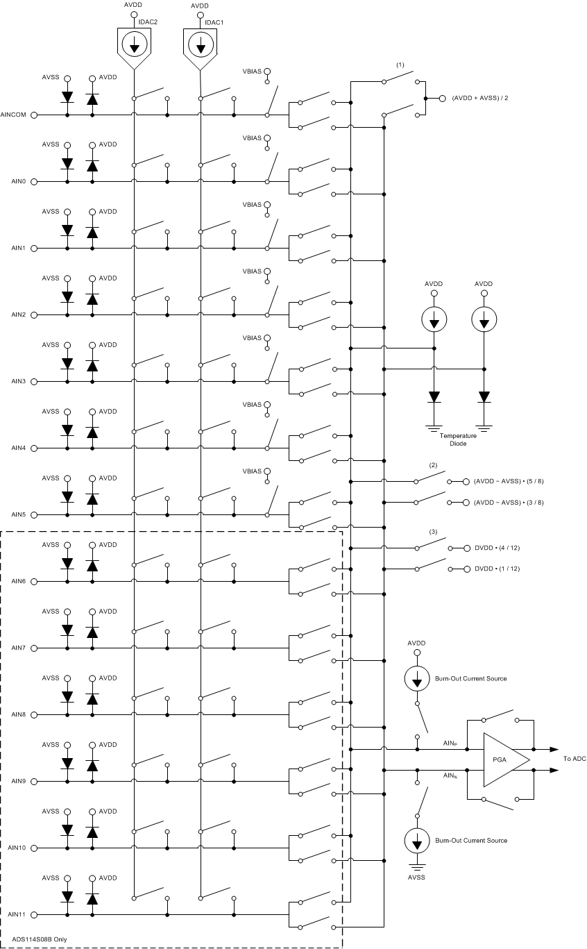
ADS114S06B ADS114S08B ai_input_mux_sbas852.gif
AINP and AINN are connected together to (AVDD + AVSS) / 2 for offset measurement.
Measurement for the analog supply equivalent to (AVDD – AVSS) / 4.
Measurement for the analog supply equivalent to DVDD / 4.
Figure 42. Analog Input Multiplexer